How to access hardware SPI port on CB2S? P16 (MOSI) GPIO breakout method
TL;DR
- A CB2S BK7231N module gets a hardware SPI MOSI breakout by wiring P16 from the QFN chip pad to an exposed pad.
- The mod removes the shield, cuts the CEN trace, solders a thin enamelled wire to the correct QFN pad, and secures it with UV-curable solder mask.
- P16 is Pin 12 on the internal IC, while CEN is Pin 21 and the module uses a BK7231N chip.
- The broken-out P16 can drive hardware SPI peripherals and individually addressable LEDs such as SM16703 and WS2812 in OpenBeken, though WS2812 still needs final fixes.
- CBU already exposes P16 on pads, so this workaround mainly helps when CB2S or similar CB3S modules are more convenient.
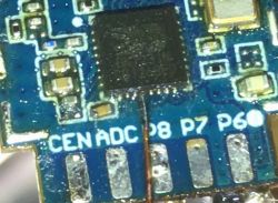
Here I will show you how to access the hardware MOSI pin, P16, on a common Tuya CB2S BK7231N module. The MOSI pin can be used for hardware SPI communication and also for driving individually addressable LEDs like WS2812 or SM16703, but it's not available on CB2S pads. We will have to solder a wire to one the QFN pads and then break it out.
Step 0: Considerations
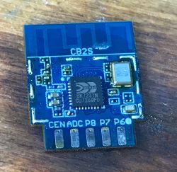
Let's consider the CB2S module:
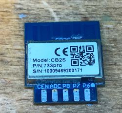
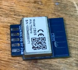
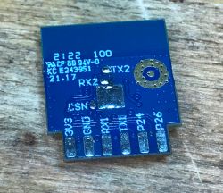
Most commonly used GPIOs are routed to the pads, there are also some debug GPIO pads at the bottom of the module, but P16 is nowhere to be found. Still, we can check the pinout of the QFN BK7231 IC itself, to find that it should be available, at least on the QFN pad:
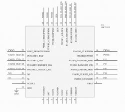
This means that the designer of CB2S module must have skipped this pin. We are going to fix that now.
Step 1: Removing CB2S shielding
Shield can be easily removed with hot air, large nozzle, and some extra flux to loosen the solder connection:
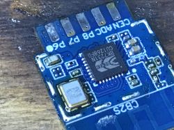
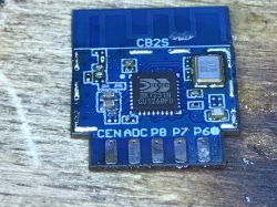
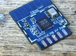
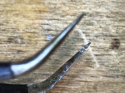
On the pictures, I have also accidentally desoldered the 100nF power supply decoupling capacitor. This needs to be fixed before using module again:
Step 2: Choosing where to route
The best option is to reuse one of the existing pads, for example CEN. I chosen to use CEN because I don't use it for flashing, I just do a power off/power on cycle and it works reliably. So, I had to cut the CEN trace:
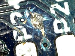
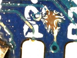
That way CEN is now disconnected from the pad and pad can be reused for our purposes.
Step 3: Preparing the wire
Get a thin wire, roughly of the size of the QFN pad. Strip the enamel from it. Tin the tip of the wire for easier soldering. You can use old broken transformer or a coil as a source of such wires.
Step 4: Soldering the wire
Once the wire is prepared, it's time to solder it to the correct pad of QFN case. Make sure that you have identifier the first pad directly - it's marked with a dot. You can use the crystal pads for orientation, just to check if you've correctly determined the orientation.
I have used a thin soldering tip for the soldering process, first I added flux and some Pb solder and then I finally made the connection:

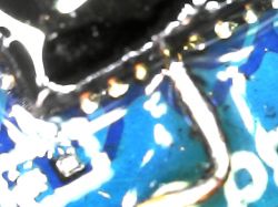
Remember to clean the PCB with IPA before going to next step.
Step 5: Adding UV-curable solder mask
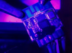
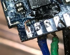
Now you can secure the connection with UV-curable solder mask. Otherwise the wire may get loose during module usage or storage. Apply solder mask and use UV to cure it:
Step 6: Second solder joint
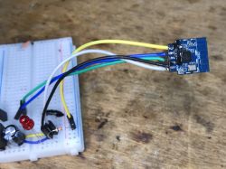
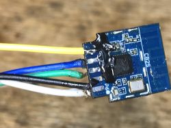
Finally it's time to solder the second end of the wire to the pad. Of course, it also have to be stripped from enamel. Then you can also solder futher wires to connect the module to the breadboard:
Summary
That way you can break out the P16 (MOSI) on the common CB2S module. The same method can also work for similiar modules like CB3S, etc. Alternatively you can look for module that has P16 already available on pads like CBU module:
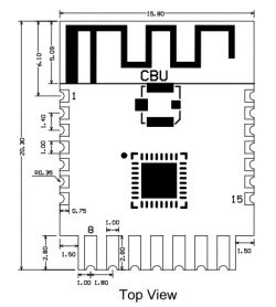
| Pin number | Symbol | I/O type | Function | 1 | P14 | I/O | Common GPIO, which can be reused as SPI_SCK (Correspond to Pin 11 of the IC) | 2 | P16 | I/O | Common GPIO, which can be reused as SPI_MOSI (Correspond to Pin 12 of the IC) | 3 | P20 | I/O | Common GPIO (Correspond to Pin 20 of the IC) | 4 | P22 | I/O | Common GPIO (Correspond to Pin 18 of the IC) | 5 | ADC | I/O | ADC, which corresponds to P23 on the internal IC (Correspond to Pin 17 of the IC) | 6 | RX2 | I/O | UART_RX2, which corresponds to P1 on the internal IC. (Correspond to Pin 28 of the IC) | 7 | TX2 | I/O | UART_TX2, which is used for outputting logs and corresponds to P0 of the internal IC (Correspond to Pin 29 of the IC) | 8 | P8 | I/O | Support hardware PWM (Correspond to Pin 24 of the IC) | 9 | P7 | I/O | Support hardware PWM (Correspond to Pin 23 of the IC) | 10 | P6 | I/O | Support hardware PWM (Correspond to Pin 22 of the IC) | 11 | P26 | I/O | Support hardware PWM (Correspond to Pin 15 of the IC) | 12 | P24 | I/O | Support hardware PWM (Correspond to Pin 16 of the IC) | 13 | GND | P | Power supply reference ground | 14 | 3V3 | P | Power supply 3V3 | 15 | TX1 | I/O | UART_TX1, which is used for transmitting user data and corresponds to Pin 27 of the IC. For the MCU solution, please refer to CBx Module. | 16 | RX1 | I/O | UART_RX1, which is used for receiving user data and corresponds to Pin 26 of the IC. For the MCU solution, please refer to CBx Module. | 17 | P28 | I/O | Common GPIO (Correspond to Pin 10 of the IC) | 18 | CEN | I/O | Reset pin, low active (internally pulled high), compatible with other modules (Correspond to Pin 21 of the IC) | 19 | P9 | I/O | Common GPIO (Correspond to Pin 25 of the IC) | 20 | P17 | I/O | Common GPIO, which can be reused as SPI_MISO (Correspond to Pin 14 of the IC) | 21 | P15 | I/O | Common GPIO, which can be reused as SPI_CS (Correspond to Pin 13 of the IC) | Test point | CSN | I/O | Mode selection pin. If it is connected to the ground before being powered on, enter the firmware test mode. If it is not connected or connected to VCC before being powered on, enter the firmware application mode. Correspond to Pin 19 on the internal IC. |
But CBU module seems to be less popular and less accessible than the CB2S/CB3S so the presented method can be useful is some cases.
The routed out P16 can be used for example for individually adressable LEDs control via hardware SPI of BK7231, which is available in OpenBeken firmware. We are currently supporting SM16703 and WS2812 also works, but WS requires some final fixes before it's fully release-ready. Let us know if you want to driver some LEDs with OBK!


Comments
Here is how you can mode CB3S module. I've cut P14 pad from the via and connected P16 to that via so I can have easier access to P16 for testing. Everything is reversable if need be. https://obrazki.elektroda.pl/3216382700_1698597352_thumb.jpg... [Read more]