
.
Here I will show how to easily run an external Flash memory with any microcontroller based on software SPI. I will discuss here the operation and meaning of the different operations (read, write, erase) and implement them in code.
The topic of using such memories seems interesting to me, to say the least, because it is very easy to get some such dice for free. They are available in many devices, I find them in old monitors, televisions, satellite TV receivers and even in computers or there laptops (it's that famous BIOS bone). It usually stores the program for the microcontroller, but I want to use it in general to record measurements and more.
Flash memory is non-volatile memory, so the data stored in it is not lost when power is removed, so you can store configurations, historical measurements and even files there.
The memories presented can most often be found in sizes of 1 Mb to 8 Mb, for example the W25Q80 or W25Q64. Note the difference between 1 Mb (megabit) and 1 MB (megabyte), where 1 MB = 8 Mb. This means that memory labelled as 8 Mb has a capacity of 1 MB.
I will make the presentation based on
OBK , but that should not matter here.
Basically we will implement what the CH341 based programmer does:
.
And we will implement this on any MCU through basic operations on the digital GPIO.
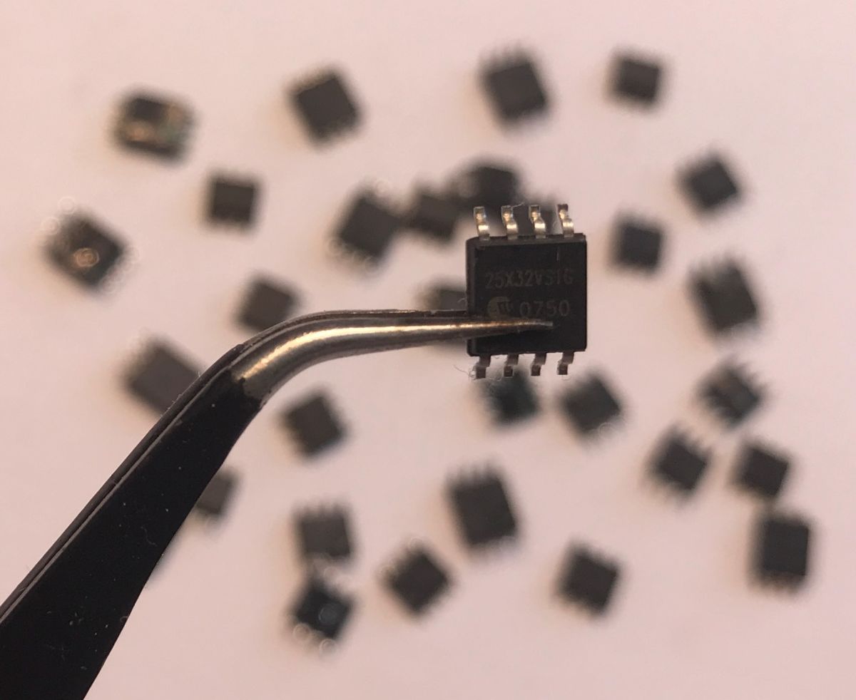
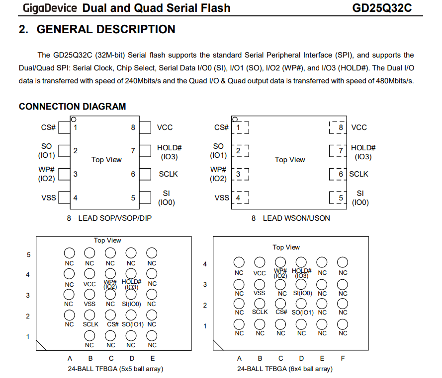
Let's consider an example memory recovered from electro-waste - the 25Q32CSIG. The name itself tells us a bit about it, as "25" stands for the SPI interface, "Q" suggests support for Quad SPI mode, "32" is its capacity - 32 megabits, or 4 megabytes, and "CSIG" is the manufacturer's and case type designations. Such a memory has 8 leads and communicates fully via SPI, making it a good candidate for our experiments.
.
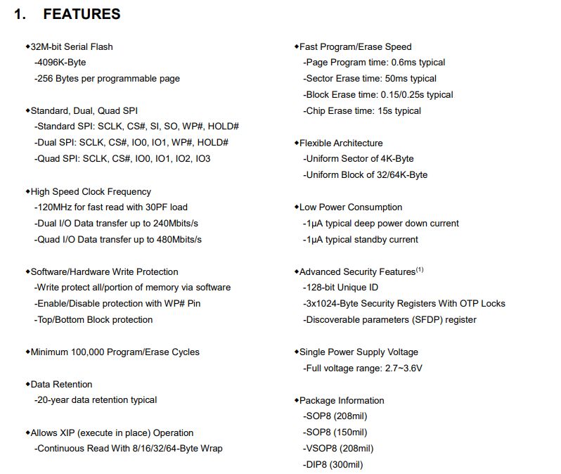
Let's review the highlights from the datasheet note. Operating voltage - up to 3.6V here, but that's not a problem as I want to run it with the MCU running at 3.3V. In addition, here we have information about the speed and endurance of the memory - a minimum of 100,000 Program/Erase cycles, I will explain this later. The data will last typically 20 years (!) and the manufacturer also gives the expected programming operation times and more. It is worth noting the information about pages and sectors, about that too in a moment.
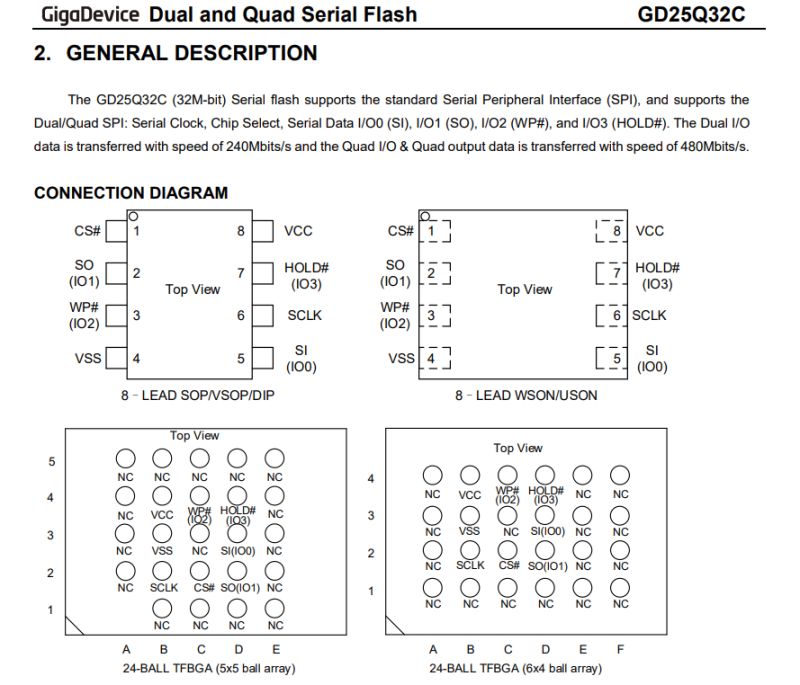
However, let's start with what can be seen at first glance. Outputs.
.
Such a memory has only eight legs, and we will actually only be connecting four to the MCU. Here we have:
- power and ground - you know, it's just worth checking the operating voltage
- SO - Serial Out (data output)
- SI - Serial In (data input)
- SCLK - clock
- CS - chip select, allows to select one of many devices on the common SPI bus (common SO, SI, SCLK)
- WP - write protect, write protection. For simplicity we will pull up a high state there, thus disabling protection and allowing writing to memory.
- HOLD - stop transmission, when we set this pin low, the memory "freezes" the SPI transmission without losing synchronisation.
That is, we ultimately only need four lines to operate: CS, SCLK, SI and SO. The rest can be left on fixed logic states (Vcc or GND, according to the datasheet).
As for the physical connection - you can use SMD to THT converter boards or solder something yourself ->
SMD to drilled prototyping board - what to do when there is no adapter at hand
Now comes the question of what we need to do with these pins. Here there are two things you need to know.
First , we have essentially three operations here:
- erase (erase) - sets the memory cells to 1 (bytes to 0xFF)
- programming (program) - sets selected memory bits to 0
- reading - simply reads the selected memory cells
This is where an important observation already comes into play, namely that if you want to write something to memory, you must first erase the section in question (more on that shortly) and then program ('extinguish') the selected bits. This may come as a surprise to people who think that there is simply writing and reading separately and that is enough. Erasing can only be skipped in one case - if you only want to extinguish bits and don't need to light them up.
Secondly , memory is organised into sections called pages/sectors and it is often these that are operated on. The Memory Organisation section talks more about this:

.
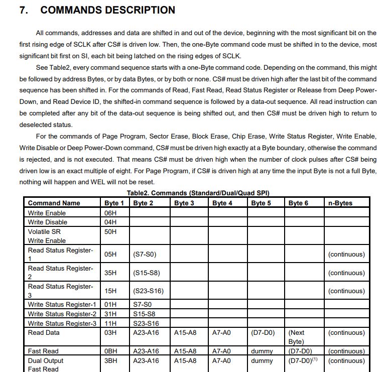
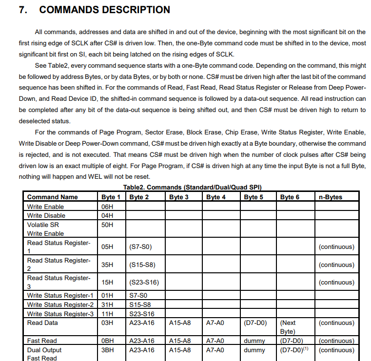
Equipped with this knowledge, we can look at the command table. These are the commands that we send through the SPI. We will only need some of them:
.
However, the commands are a bit much, so I have prepared for you a selection of the bare minimum that I think is needed for operations on such memory.
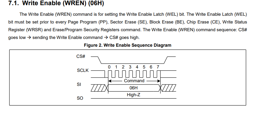
1. setting the Write Enable bit (0x06, write enable):

.
Setting the Write Enable Latch (WEL) bit is necessary before any page programming operation and before erase operations.
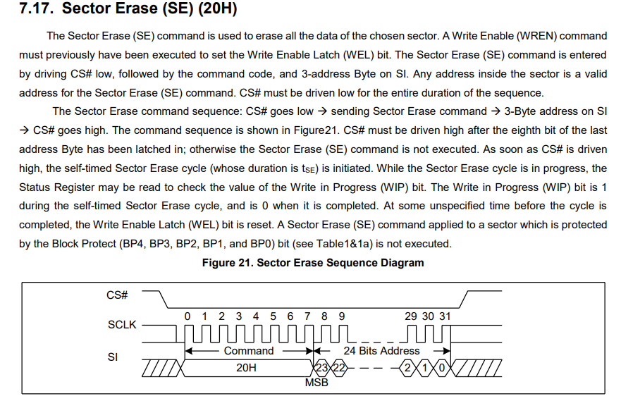
2. memory sector erase (0x20):

.
The command requires 3 bytes addressing the sector. The deletion starts when the CS is raised. No further operations can be performed at that time, it is necessary to check the Write In Progress bit of the Status register to find out when the operation completes.
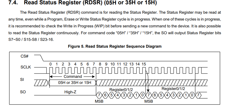
3. read the Status register (0x05):

.
This is the Status register check mentioned above.
4. page programming (0x02):
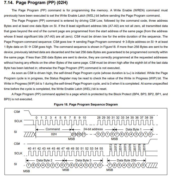
.
Page programming allows bits to be extinguished within a page, although the address itself can point anywhere in the page. You only need to divide the Program commands so that they apply to one side,
no 'crossing' the boundary to the other side is supported . This programming is not able to "light" the bits, only can "extinguish" them, which is why it is usually preceded by an erase cycle.
5 Read (0x03):
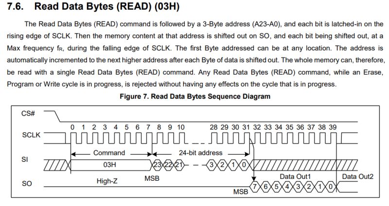
.
Read is the simplest command. The entire memory can be read in with one read, it does not need to be split.
It's time to move on to the implementation. .
I'm assuming a basic knowledge of SPI here, but I'll show the implementation from my environment anyway. The whole thing is done programmatically based on bit-banging. First the structure - the GPIO indexes:
.
Implementation:
.
Here we have in sequence:
- SPI_Send() - a function that sends a byte through the SPI, bit by bit from the most significant bit. After each change of the MOSI line a clock pulse is generated
- SPI_Read() - a function to receive a byte through the SPI. Each bit is read after the clock is raised and folded to a full byte
- SPI_Begin() and SPI_End() - simple functions managing the CS (chip select) line, activating and deactivating the flash memory respectively
- SPI_Setup() - preparing the GPIO pins: setting the appropriate directions and initial states
It is worth noting that HAL_PIN_... is a hardware abstraction - in my case it is associated with the GPIO of a particular microcontroller. In your case it could be another library or direct manipulation of registers. In Arduino, you can simply give the famous digitalRead and digitalWrite there.
Based on this interface we can already write higher level functions - e.g. flash_write_enable(), flash_erase_sector(address), flash_read(address, buffer, length), etc. But before we get to that, it's still a good idea to check that the memory is working - that is, to read its ID.

.
This is what we will do in the next step - read the JEDEC ID (command 0x9F), which allows us to confirm that the chip is working, that the lines are well connected, and that SPI communication is running correctly. This also makes it easy to detect errors in connections or GPIO configuration.
We already have the SPI functions defined and we already have the communication flow shown in the figure from the datasheet note. All we need to do is put this into the code:
.
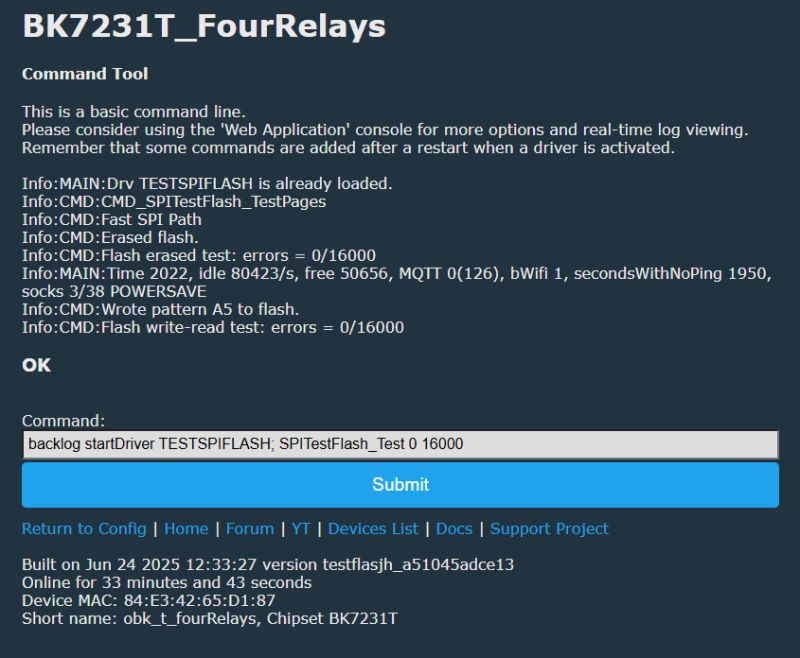
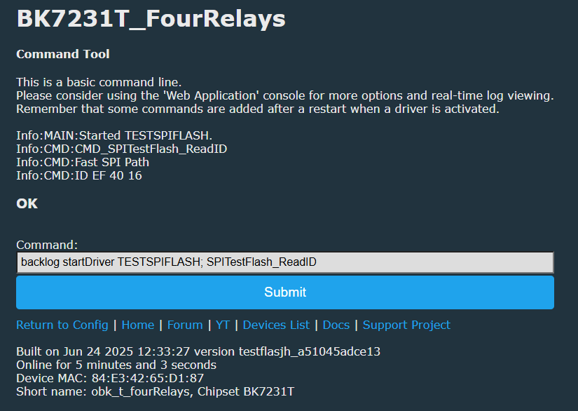
In my case it worked out as above. I still added a command to call this from the control panel:
.
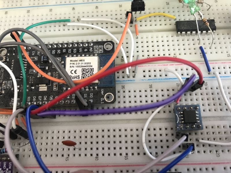
My test bench - the memory is soldered to the DIP size converter board:
.
Test results:

.
The ID reading works - we received EF 40 16. This can now be interpreted.
- EF - Winbond Electronics (manufacturer)
- 40 - chip family (here means standard SPI NOR Flash series)
- 16 - chip capacity, in this case 0x16, which corresponds to 32 Mbit, or 4 MB
This result confirms that we are dealing with a W25Q32 chip - as I wrote. This means that the connections are correct, the SPI is working properly and the chip is responding to commands.
Now we can implement the remaining commands. Waiting for the operation to complete:
.
The above code reads the status register in a loop and checks if a particular bit of it is off. If it is not extinguished, it waits a short moment (longer with each iteration) and performs the read again. At this point, I have not given there a protection against a possible loop without output.
Sector deletion:
.
The code above simply sends the sector erase command in question along with the address and then waits for it to be executed.
Notation (including page division):
.
The above code works in accordance with the documentation of the Page Program 02H operation, i.e. it respects page boundaries and splits the sent data accordingly. This allows us to send any sequence of bytes and it will still be programmed correctly.
Memory reading:
.
There is no major problem here. You can read everything in one block.
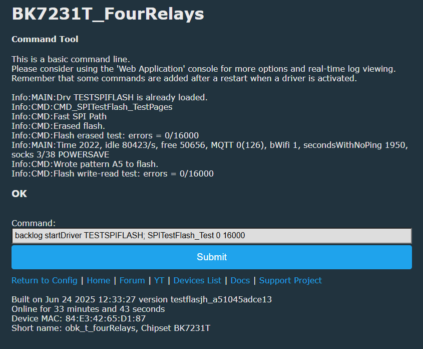
Based on these functions, I have prepared a short method to test the memory in a selected range:
.
The method takes as argument the address, the number of bytes and the reference byte. At first, the required number of pages is deleted, then the deletion is verified, and then the memory is programmed with the specified byte. Finally, the readout verifies what we have programmed.
.
Such method makes it possible to fully check the correctness of the communication, including the division of the record into pages.
Finally, only one question remains -
is it possible to somehow set only the byte of our choice to a given value ?
Basically there is no such
direct option here. The Page Program command allows us to extinguish any bits, but does not give us to light them. In a situation where we want to fuse one of the bits, we have to read the entire sector (4KB), store it in RAM, perform an erase on it, and then modify it in RAM and upload it again.
Is it that bad though? It depends, this can also be used to optimise memory consumption. Memory is consumed by erase cycles, and nobody says that every write of a few bytes has to mean an erase.... you can isolate, for example, a structure of 64 bytes and write it to a page of size 4096 all 64 times, on consecutive memory cells, and when reading it only cleverly check which is the current one. This could be useful for writing small amounts of data that are frequently changed.
To summarise , flash memory with SPI interface is very simple to set up. You don't need a lot of code for it at all, nor do you need external libraries. You just need to implement a few basic operations and be aware of the limitations of such a memory (requirement for sector erase) to be able to use it to write data from your own program.
The only question that remains is what kind of data and what about deleting in practice - I will try to show this in the next part. Separately, I will also try to optimise the software SPI so that each transaction takes significantly less time.
Do you use extra Flash memory bones in your projects? .
PS: This is not the end of the Flash memory adventure - there are at least some more parts planned:
- Manual recording of measurement results in Flash memory (weather station?).
- Optimisation (reduction) of erase cycles (one erase cycle per many writes of a small data structure)
- Optimisation of bit-bang by skipping HAL and writing directly to registers on BK7231
- Running a miniature LittleFS file system on an external 8 Mb Flash bone


Comments
. How much memory does such a read and write procedure take up after compilation? [Read more]
It depends on many factors. I've tested it so far for this situation: - a newer version of the SPI software support code (bit-banging with direct register writing, but expanded loops, etc) - the initial... [Read more]