Nearly every electronic device intended for commercial use is subject to electromagnetic compatibility (EMC) tests. Each company planning to sell its products in a given country must ensure that the product has been tested for compatibility in accordance with the requirements introduced by the national regulator of that country. In the USA, the regulations governing the principles of testing devices for electromagnetic compatibility are established by the Federal Communications Commission, based on guidelines and detailed procedures developed by CISPR ( International Special Committee on Radio Interference ) and IEC ( International Electrotechnical Commission ).
To legally sell products, an electronic product sample must pass a series of detailed tests. In many cases, manufacturers carry out the appropriate tests themselves and declare that the device meets the requirements of the relevant standards, but must have a detailed report showing the conditions and results of the measurements performed. Many companies choose a different path, commissioning such tests to specialized laboratories that have the necessary accreditation. Measurements checking whether a given product meets all the requirements described in detail in the applicable measurement specification of devices are called compliance tests.
Full compliance tests strictly follow the guidelines and settings, and their results can be the basis for issuing a certificate of compliance of the device with the requirements of the test procedures. However, this type of testing can be costly and may require a specialized test environment and hardware that may not be available for many companies.
One method of reducing the additional costs associated with ensuring that a designed circuit complies with electromagnetic compatibility (EMC) standards is to perform compatibility measurements throughout the design process, before sending the finished device for full compliance testing. Such pre-certification tests can be very cost effective and can be performed in such a way as to come closer to the conditions used in conformity testing. Such measurements will increase the certainty of passing the compliance tests the first time, reduce the costs associated with these tests and accelerate the product launch.
We will discuss pre-certification test methods that can be used to locate potential EMC problems in the circuit under design. Our goal is to make it easier for the reader to learn about the EMI / EMC tests used in the world using simple tools and measurement methods.
Radiated disturbance measurements / measurementsclose fields
A non-intentional radiator is a device that generates radiation in the RF band resulting from its construction or constituting a side effect of its operation. Put simply, a non-intentional radiator is very similar to a radio transmitter transmitting noise on many radio channels simultaneously. Such radiation can adversely affect other devices that receive such unwanted signal.
One of the basic tests is the measurement of radiated emissions by the product with the spectral analyzer with the antenna placed a few meters from the device under test. This test is called far-field radiated emissions measurement, and its block diagram is shown in Figure 1.

Figure 1: Simplified block diagram of the radiated emissions test.
In this test, we simply connect the antenna to the spectral analyzer and measure the input signal in the desired frequency range. While the idea behind measurement is simple, there are a few major measurement considerations to keep in mind:
1) Most antennas are broadband. This means that they perceive a wide range of frequencies and do not distinguish signals from sources outside the measured area from the actual signals of the tested device. For this reason, any measurements made via the antenna are very sensitive to other RF signals, such as signals from radio stations, WiFi, etc.
2) Also other environmental factors (metal shelves, desks, people, etc.) adversely affect the measurements. This is due to reflection and absorption of signals in the environment, which makes accurate and repeatable measurements almost impossible.
Similar equipment is required to successfully conduct complete radiated emission tests, but they also require a test rig where the radiation level of external RF sources that could interfere with the measurements is very low. The so-called open measuring fields Open Air Test Facilities ) are generally located in geographic areas that have minimal radio signals, such as the open prairie in central North Dakota, USA.
Open measurement fields were very popular in the 20th century, but their number has decreased significantly due to the sharp increase in the number of external RF signal sources. In those days, most RF signals was produced by AM or FM radio transmitters and open measuring fields could be located in areas without a large amount of interference signals. Currently, we have WiFi, Bluetooth transmitters and mobile phones - radio radiation is present everywhere.
Therefore, other solutions were needed, which appeared in the form of special measurement chambers that suppress external RF signals and minimize reflections of internal RF signals. Such anechoic or semi-reflective chambers fulfill this function, but they cost a lot. A small semi-anechoic chamber measuring just over 1m x 1m can cost over $ 50,000. In most cases the cost is too high for rarely performed measurements.
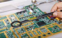
Probing of nearby electromagnetic fields is a measurement technique that uses special measuring probes to minimize the influence of RF radiation from the environment. Nearfield probes typically have two design solutions. Magnetic field probes, or H-field probes, have loops that couple the probe to the magnetic fields generated by time-varying currents. Both structures are very sensitive to the distance from the radiation source. To ensure effective measurement, even with a very sensitive analyzer or a connected preamplifier, the probes must be located at a maximum distance of several centimeters from most of the tested radiation sources.
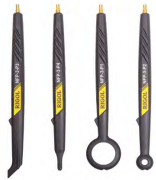
Figure 2: Rigol EMC probes. The loop-terminated probes are H-field probes. The smallest-terminated probes are the electrical component of the field (E-field).
The simplest test is to configure the spectral analyzer to work with the peak detector and the RBW filter and sweep range settings covering the area standardized by the regulator's requirements for a given device. Then select the H or E probe appropriate for the structure under study and move it over the entire surface of the perimeter (device).
The orientation of the probe in space (angle, distance) is also important. The probes work like an antenna, capturing radiation from welds, housing openings, tracks, and other circuit elements that may emit RF signals.
A thorough scan of all circuit components, connectors, knobs, housing openings and welds is essential. Figure 4 shows the use of an H-field probe for testing the emitted radiation.
For the first test, set the peak detector on the spectral analyzer. This will detect the "worst case" of RF radiation reading and is the quickest way to locate potentially problematic areas. Larger probes allow faster scanning speeds, albeit with a lower spatial resolution.
Now that you have an understanding of the problem areas, you can get more detailed information using some common techniques. If possible, choose a spectral analyzer that has the standard configuration used in full compliance testing. These include: quasi-peak detector mode, EMI filter, and bandwidth (RBW) settings conforming to the full compliance test requirements for the product under test.
This type of setup will extend the measurement time, but should be used in problematic areas. Such settings are used in the full compliance test, therefore pre-certification measurements in the same configuration will provide a greater degree of visualization of the electromagnetic disturbance characteristics of the tested structure.
The memory of many instruments can keep the correction factors for cables and antennas, which allows the observation of a clean signal, without additional errors introduced by the equipment.
The next step of the emitted interference test procedure is the use of antennas instead of near field probes, a rotating table for the tested equipment (EUT - Equipment under Test ) and, if possible, performing tests in a special room that minimizes the influence of environmental factors (the so-called semi-anechoic chamber). A detailed description of such measurements is beyond the scope of this study.
Measurements with a set of near field probes
Emission testing at the PCB level can be performed with a spectral analyzer such as the Rigol DSA815 (9 kHz to 1.5 GHz), a near electric field (E) probe, a near magnetic field (H) probe, and appropriate interconnecting cables.
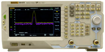
Figure 3: Rigol DSA815-TG Spectral Analyzer.
To operate the spectral analyzer with near-field probes (shown in Figure 2), a 50 ? cable terminated with N-type plugs (analyzer side) and SMB plugs (probe side) is required.
You can also build your own probe from a not too stiff RF coaxial cable. After removing the outer coating of the cable and insulator several centimeters long, the cable should be coiled into a loop and immersed in Plasti Dip or other special liquid insulating mass. Larger diameter loops will pick up smaller signals but will not have the spatial resolution of smaller diameter loops.
For the first test, set the peak detector on the spectral analyzer. This setting ensures that the instrument captures the "worst cases" of peak RF emissions. This is the fastest way to locate the problematic spots, as it allows you to waste the least time in one place scanning the entire perimeter. Larger probes allow faster scanning speeds, albeit with a lower spatial resolution. Smaller probes, such as E-field probes, provide excellent spatial resolution and can be used to detect RF radiation on single leads of circuit components.
The orientation of the probe in space (angle to the perimeter plane and distance from the perimeter) is also important. The probes work like an antenna, capturing the emitted RF radiation. Positioning the probe loop as perpendicular to the magnetic field force lines as possible (highest H field strength) maximizes the signal strength at the probe output.
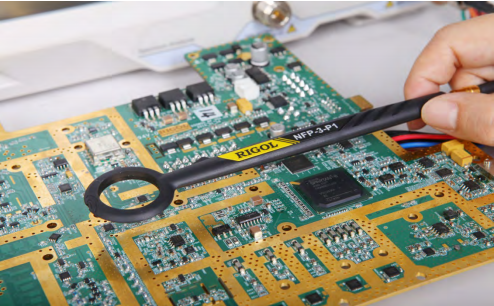
Figure 4: Example of using an H-field probe and spectral analyzer to locate points suspected of excessive interference emission. Note the orientation of the probe tip.
Care should be taken to scan the welds of screens and covers, openings, paths and other items that may emit RF radiation. Accurate scanning of all circuit components, connectors, knobs, housing openings, and shield can welds is critical in identifying potential locations in the circuit where RF radiation may "leak" to the exterior of the device housing.
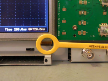
Figure 5: Measurement of the emission of the shield ribbon cable with the H-field probe.
Aluminum foil or conductive tape may be used to cover areas that may be a potential emission source, such as vents, covers, conduit, screen joints, or cable entries through the enclosure. Test these places without foil or tape, then cover them and repeat the probe scan.
Once problem areas have been identified, more detailed information can be obtained using several common techniques. If possible, choose a spectral analyzer that has the standard configuration used in full compliance testing. These include a quasi-peak detector, EMI filter, and bandwidth (RBW) settings that conform to the full compliance test requirements for the product under test.
This type of setup will extend the measurement time, but should be used in problematic areas. Such settings are used in the full compliance test, therefore pre-certification measurements in the same configuration will provide a greater degree of visualization of the electromagnetic disturbance characteristics of the tested structure.
Tips
A spectral analyzer with near field probes can be useful tools for locating problems with electromagnetic interference (EMI) emissions.
- When working with the H-field probe, try different orientations in space to isolate emission points.
- Be sure to test all shield welds, and the contact points of the housing surface, and complete the grounding and shielding effectiveness test.
- Openings in the housing or shielding boxes emit radiation similar to solid structures. They work like antennas.
- Ribbon cables and input cables / sockets with poor screening and incorrect grounding are well known causes of radiated emissions.
Conducted electromagnetic interference measurements
Measurements of conducted EMI disturbances require the analysis of radio frequency energy that passes from the device or the circuit under test to the low-voltage power grid supplying this device / circuit. RF signals flowing back into the power line can cause interference in the AM radio signal transmission bands. To minimize such interference, it is important to quantify the RF power and frequency that the device produces when connected to mains.
Like radiated EMI disturbances, conducted disturbances are also measured with a spectral analyzer, but additionally a surge arrester and a network impedance stabilization system (LISN) are required. Line Impedance Stabilization Network ). The LISN circuit isolates the mains from the equipment under test, cuts off all interference generated by the EUT, and interconnects the signals generated by the EUT with the input of the spectral analyzer.
As with the emission tests, it is best to start by scanning the entire required band with a peak detector with the analyzer. A scan is then performed with a quasi-peak detector to increase the confidence and accuracy of the measurements.
Configuration of conducted emissions measurements
The more the measurement system is compatible with the configuration of full compliance tests, the more data obtained will be closer to the results of compliance tests performed by the certification laboratory. But this is not always practical.
The following block diagrams show the standard recommended electrical and physical configuration of the test bench.
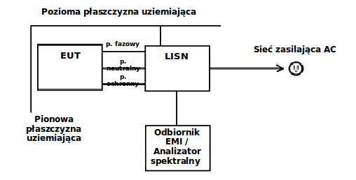
Figure 6: The electrical circuit of the conducted emission test bench.
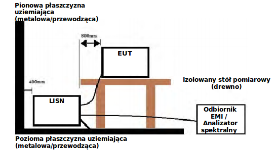 [/url]
Figure 7: Physical layout of the stand for measurements of conducted emissions.
Key Issues:
1. The vertical and horizontal ground planes are typically sheets of metal twice the size of the equipment under test (EUT).
2. The vertical and horizontal ground planes should be electrically bonded together and grounded.
3. The tested device must be placed on an insulated table above the horizontal shielding plane. No devices or cables may be between the EUT and the horizontal ground plane.
4. The LISN is electrically bonded to the horizontal ground plane. LISN is a network impedance stabilization system. Its task is to separate AC disturbances from the conducted disturbances generated by the EUT. The LISN system with rated voltage, current and frequency should be selected appropriately to the device under test.
5. Make sure that all connecting cables lie freely and do not form coils and thus induction loops.
6. The spectral analyzer should be located at a distance from the horizontal ground plate, typically not less than 1 m.
Test procedure
After setting up the test bench and connecting the LISN system to the ground planes, turn on the analyzer for a minimum of 30 minutes before starting the tests to achieve maximum stability and accuracy.
Configuration of the spectral analyzer
- Option: If your analyzer has the ability to set the quasi-peak detection and FCC resolution bands of 200 Hz, 9 kHz and 120 kHz, you can use these to obtain data that will more accurately represent the data collected during actual compliance tests. note that quasi-peak detectors take much longer to complete the scan of the required frequency range.
- Set the band of the RBW separation filter.
ATTENTION: The bandwidth is determined by the standard and the type of tested device. For example, the FCC subpart-15 specification sets the RBW band to 9 kHz when testing the EUT in the 150 kHz - 30 MHz band.
Check national regulations for standards specifying EMC tests applicable to the device under test.
ATTENTION: Many specifications give limits in dBuV or in V.
Optional: If the analyzer is capable, set the amplitude scale to V.
ATTENTION: Some analyzers have a pass / fail selection function that allows you to set the upper limit line. This can be useful when evaluating the spectrum against the limits set by the EMC standard against which the test is performed.
Any boundary lines can be stored in the internal memory of the analyzer.
- Set up the positive peak detector on the analyzer. Positive Peak ). This detector will show the highest values, or "worst case" values, in the pre-certification testing.
- It is recommended to include a transient limiter and an external 10 to 20 dB attenuator in the analyzer input circuit to minimize the probability of damage to the instrument's sensitive input circuits. The attenuator protects the analyzer input circuits from unknown signals that could damage the instrument. It is also used for convenient control of possible overload after checking the background noise spectrum.
The spectral analyzer has protection circuits, but its input may show transient states (disturbance pulses) too fast for the protection to trip.
- Set the start and end frequency values specified in the EMC standard applicable to the device under test.
- Set the RBW filter band in accordance with the value specified in the EMC standard applicable to the device under test.
Background noise control
- Apply power to the LISN system.
- Connect the analyzer to the output of the LISN system.
- Scan the required frequency range with the peak detector and the input attenuator set to 10 dB.
Peak value test
- Disconnect the analyzer from the LISN system.
- Connect the devices under test (EUT) to the LISN.
- Reconnect the analyzer to the LISN system. This procedure allows to minimize the risk of damage to the analyzer by the appearance of transient states at its input.
- Observe the conducted emission spectrum and set the attenuator attenuation value to 20 dB. If the curve on the screen does not change with different attenuation values, it is likely that the analyzer input is not overloaded and the measurement quality will be high. Pre-certification tests can be continued.
If the spectrum changes value with different attenuator settings, it is likely that the input is overloaded with wideband power and additional attenuation is required. You can compare spectra for 20dB, 30dB etc. until you get a spectrum that will not be subject to changes.
The smallest attenuation value should be selected at which no errors resulting from input overload are visible.
In the worst case, it will not be possible to test the EUT with a spectral analyzer. You will need to use a typical EMI receiver with preselection filters
- Observe the spectrum of conducted emissions and look for frequency fringes that exceed the pre-set cut-off lines. Record the values of these frequencies.
Quasi-peak scanning
In the next step, you should scan in detail the frequencies that have exceeded the limits in the previous test.
- Adjust the analyzer center frequency sequentially to frequencies exceeding the limits.
- Select an appropriate RBW band and set a sweep range equal to twice the RBW bandwidth.
For example, if the excessive emission peak is 10 MHz and the RBW is set to 120 kHz, the center scan frequency must be set to 10 MHz and the sweep range of 9.88 MHz to 10.12 MHz.
- Optional: Change detector to quasi peak (QP).
ATTENTION: The operation of the quasi-peak detector is based on the charge and discharge times of a standard resonant circuit. This type of detector requires 3 times the scanning time than the peak detector. Therefore, it is best to use quasi-peak scanning only at small sweep ranges.
- Compare the obtained results with the permissible limit values for the given frequency.
- It is recommended to keep the conducted emissions 10 dB below the specified limit.
- It is also recommended to compare the obtained results of the pre-certification tests and measurement configuration (test bench, measurement procedure, measurement equipment settings) with the configuration used by the certification laboratory that will test the EMC compatibility of your product. Doing so will help identify problems in self-certification tests. Careful comparison will save you money in your pre-certification test budget and will increase confidence in your own test results.
Interference immunity tests
Products containing electronic circuits can be sensitive to radio interference. Devices exposed to RF interference may be prone to malfunction or malfunction. Products that are harmed by exposure to radio frequency interference are known as susceptible to interference, while products that do not exhibit problems in the presence of radio interference are known as noise immunity.
Radio interference can cause:
- Rearrange / mix screen information.
- Slow down, freezing or blocking (no response to the operation of keys, buttons) of the device.
- Falsifying or distorting data.
- System reset or restart.
Thorough design analysis, including component selection, shielding, and cable selection is the first step to creating a product that is capable of "as expected" performance with a specified RF interference level, but early testing under real environmental conditions is the only sure way. determining whether the developed structure is sensitive to problems related to RF interference
In the following paragraphs we will try to show how the RF generator and some simple tools allow you to identify the weaknesses of the product design.
Susceptibility to radiated disturbances
Tests of susceptibility to radiated disturbances consist in observing the operation of the tested device (DUT) in the field of influence of a known source of RF signals. The signal is provided to the DUT using either antennas for far field tests or near field probes for motherboard level tests.
defines the frequency range of the test signals as 80-1000 MHz. Such signals may be amplitude modulated with a sinusoidal signal with a frequency of 1 kHz with a modulation depth of 80%. The modulated signal helps to quickly identify current rectification phenomena in sensitive circuit components.
For far-field tests, an RF signal source, such as the Rigol DSG3000 or DSG800 generators, is connected to an antenna positioned a meter or two from the DUT. Source RF it is then configured to generate a signal with 80% AM modulation and a modulation frequency of 1 kHz. The amplitude should be set as high as possible and the carrier frequency may be set e.g. to 9 kHz.
ATTENTION: The DUT should be configured to run in the most used state. All cables (power, I / O, etc.) should be connected and in place. Cables can act as antennas and thus can directly affect the operation of the device.
Observe the DUT for any changes in operation or problems such as interference or noise on the screen. Then gradually increase the carrier frequency of the test signal and observe the operation of the DUT, recording the carrier frequencies at which problems occur and the nature of the problems. When the tests are completed when reaching the 1 GHz frequency, you can rotate the device under test in relation to the transmitting antenna and repeat the test procedure if a more thorough test is required.
ATTENTION: Generated antennas should only be used in a shielded anechoic or semi-anechoic chamber so as not to interfere with broadcast and emergency service bands. Broadcasting a radio signal over a wide frequency range is illegal without the appropriate license.
The use of Rigol's instruments for testing, such as the DSG3000 or DSG800 series generators, provides great flexibility in setting the wavelength, power and modulation of the output signal, which helps in the quick identification of EMC problems of the product.
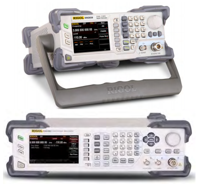
Figure 8: RF signal sources - Rigol DSG800 and DSG3000 generators.
Near field tests are helpful as they do not require special test chambers. The E-field and H-field probes produce high-intensity fields less than 3 cm from the probe tip and thus do not cause problems with interfering with broadcasting and emergency services systems. At the same time, their small size allows the RF signal to be fed directly at specific points in the circuits.
A commercial example of a near field probe is the Rigol EMC probe kit shown below.
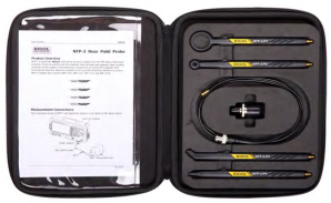
Figure 9: Rigol EMC probes. The loop-terminated probes are H-field probes. The smallest end is the E-field probe.
In the near field tests, the RF signal source is configured the same as in the far field tests, but this time the tip of the probe (acting as an antenna) is placed very close to the circuits or components on the board of each carrier frequency of the test signal. By scanning the entire board surface, observe the DUT and be sure to check for any suspected problem points, especially near sensitive analog circuits.
In the test shown in the photo below, we removed the shielding can covers from the oscilloscope motherboard and used an E-field probe powered by a DSG3000 generator to output RF signals. for sensitive analog input circuits. As can be seen from the screen view (Figures 11 and 12), with the RF shielding cans removed, the RF radiation deforms the input data and significantly changes the shape of the displayed waveform.
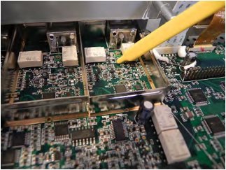
Figure 10: Using a near field probe in an unshielded analog oscilloscope input circuit.
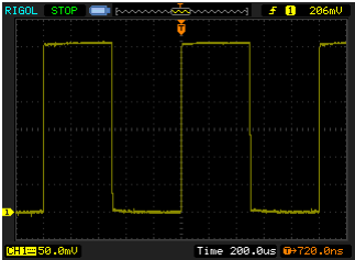
Figure 11: Signal on the oscilloscope screen with shielded input circuits.
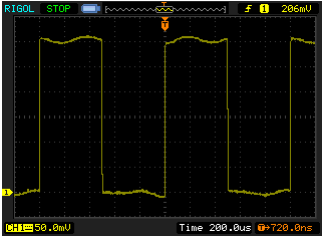
Figure 12: Signal on the oscilloscope screen with the input circuit screen removed.
Additional tests
Another useful test is to apply RF signals to cables connected to the DUT using an RF source and a current probe. Cables can also function as a receiving antenna and couple unwanted signals to the device under test. With such a measurement system, it is possible to check the susceptibility of the circuit to external RF disturbances penetrating through the connecting cables by stepwise changing the generator frequency in the entire required frequency band. Commercially available current probes can be used, but an acceptable probe can be built by yourself using a snap-on ferrite core, a few turns of insulated wire, some epoxy glue, and a BNC socket. An example of such a probe is shown in Figure 13.
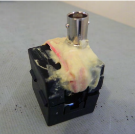
Figure 13: Homemade current probe.
To perform this test, connect all cables to the device under test as in normal operation. Configure the RF source for generation with the maximum AM signal strength, such as that used in the previous tests (modulation depth 80%, modulating frequency 1 kHz), clip the probe on the tested cable and observe the operation of the DUT. Carry out such observation for different carrier frequencies. Continue the test until the desired maximum frequency is reached, then repeat the procedure for each cable connected to the DUT.
ATTENTION: Tests with the current clamp probe should be performed only in a shielded anechoic or semi-anechoic chamber, so as not to interfere with broadcast communication bands and emergency services bands.. Broadcasting a radio signal over a wide frequency range is illegal without the appropriate license.
To demonstrate the use of the current probe, we performed an experiment on a USB bus powered demo board. We used a DSG3000 generator and a home-made probe fastened to a USB cable connected to the board without a filter, and we observed its output signal.
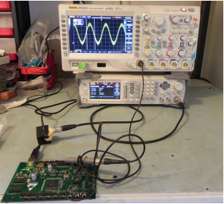
Figure 14: Magnetic coupling of RF frequency into a USB cable without a filter choke.
With no RF frequency on the cable, the screen was smooth.
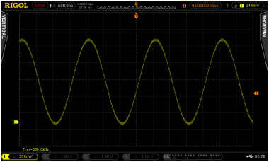
Figure 15: Sine wave from demonstration board without RF interference.
After turning on the RF signal, the board's waveform started showing signs of distortion. The strongest interference appeared at the 110 MHz carrier frequency, as shown in the figure below.
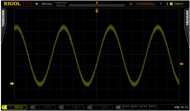
Figure 16: Distorted sine wave output with noise
at 111.1 MHz due to interference with the USB cable.
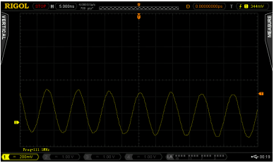
Figure 17: A section of the waveform showing the disturbance details, enlarged by the Zoom function.
In conclusion, a source of RF signals such as the Rigol DSG3000 or DSG800 generator and a few simple tools will enable independent testing of the designed device's resistance to interference at an early stage of design works, saving the company's time and money.
Sponsored article
Permission to publish // gulson


