Sometimes turning your PCB designs into reality can be costly, especially when dealing with high-layer PCBs. However, at JLCPCB, we provide an economical solution - a once-a-month opportunity for every customer to partake in 6-8 layer PCB prototyping at no cost, and now we sincerely invite you to come and experience it with us.
*JLCPCB also offers a special price of $2 for 1-8 layer FR-4 PCBs (50mm*50mm, 5 pieces) to alleviate the cost burden during project development, enabling innovative ideas to flourish under more favorable conditions. To save more, sign up on JLCPCB official website and get up to $54 off register coupons.
How to Experience Monthly Free 6-8 Layer PCB Prototyping
To enjoy the once-a-month free prototyping, your PCB order needs to meet the following criteria:
• Layer: 6 or 8 layer
• Size: Within 50mm*50mm
• Quantity: 5 pieces
• PCB Specifications: Default settings
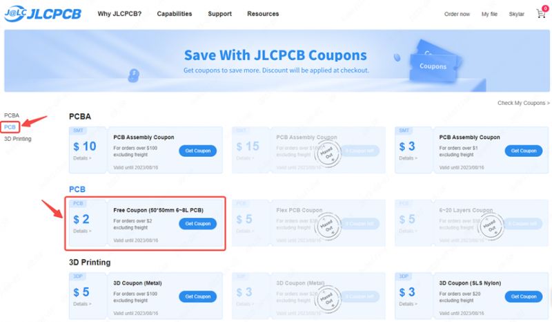
To start, you will need to visit the JLCPCB Coupon Center and claim a $2 coupon for 6-8 layer PCBs. Each month, we release one such coupon in the Coupon Center. Remember to claim it before placing your order.
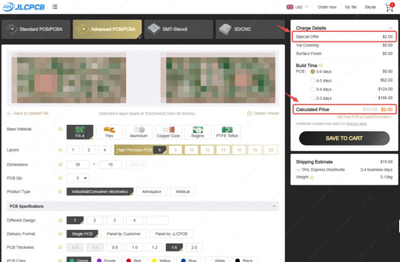
Next, upload the Gerber file that meets the requirements for free prototyping to the quotation page.
Once uploaded successfully, the pricing section on the right side will display the $2 special price for your order. Click "Save to cart" to proceed to the shopping cart.
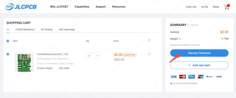
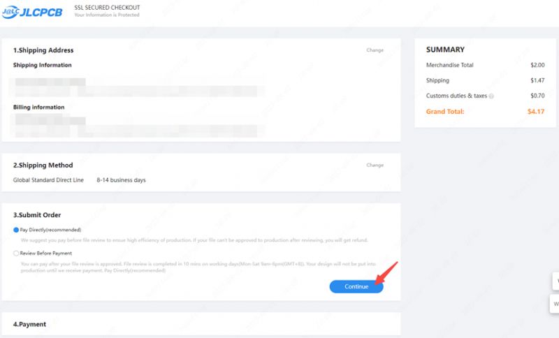
Click "Secure Checkout" in the cart, then fill in the shipping address and select the appropriate shipping method. If you prefer to pay the bill directly, then click "Continue" to proceed to the payment step.
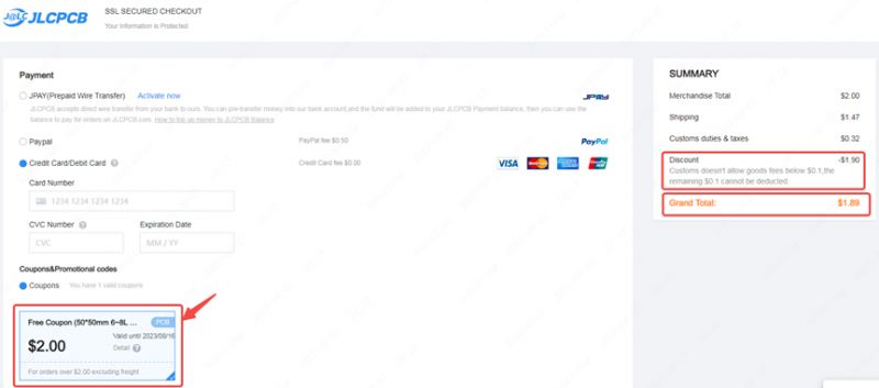
During payment, apply the $2 coupon you claimed for 6-8 layer PCBs to avail of the discount. You will see that the product cost has been deducted. (In this case, the total price is deducted from $4.17 to only $1.89) Congratulations! You have successfully secured an opportunity for free 6-8 layer PCB prototyping.
Please note that if you select parameters outside the special offer range, such as choosing a panel as the delivery format, a soldermask color other than green, a thicker outer/inner copper weight than the default setting, or if your PCB size exceeds the 50mm*50mm limit for the special offer and you need more than 5 pieces, regular charges will apply.
However, even if your order doesn't qualify for the special offer, rest assured that our regular prices are still favorable. We have made some additional discounts for high-layer PCBs:
• No longer additional charges for via-in-pad for 6-20 layer PCBs.
• For 6-layer PCBs within 10cm*10cm (5pcs) and within 5cm*5cm (10pcs), the price has been reduced from about $85 to $60-63, and the engineering fee adjusted from over $100 to $60 (board thickness within 2.0, 2.0 not included).
JLCPCB High Layer High Quality
With such a discount, can the quality of PCBs be maintained as always? The answer is "Yes"!
At JLCPCB, we deliver cost-effective PCB manufacturing solutions without compromising on performance, durability, and reliability. Backed by our 5 intelligent production bases, we continuously strive for improvement. Through continuous efforts, we've optimized processes, enhanced PCB production layouts, and implemented a comprehensive automated intelligent management system. These initiatives have yielded promising outcomes, also for 6-8 layer PCBs production. Additionally, as our production volume keeps expanding, we can significantly reduce costs because of the large-scale effect on production, allowing us to pass on the savings to every customer. At JLCPCB, we aim to share our years of PCB manufacturing achievements with engineers and makers, giving them a competitive edge by leveraging our production advantages.
JLC's Commitment to PCB Manufacturing
• JLCPCB guarantees full-film PCB manufacturing, without resorting to negative film.
• Via-checking with four-wire low resistance is ensured for all boards.
• High-precision LDI is employed on multi-layer boards(including 4-layer PCBs), for a stable and reliable solder mask bridge.
Before delivering the PCBs to customers, we conduct at least three quality checks:
• Automated Optical Inspection (AOI)
• Flying Probe Testing
• Final Quality Checking piece by piece before shipping
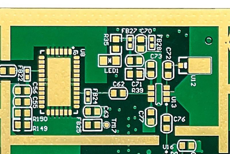
A Peek of JLCPCB multi-layer PCBs with ENIG & via-in-pad
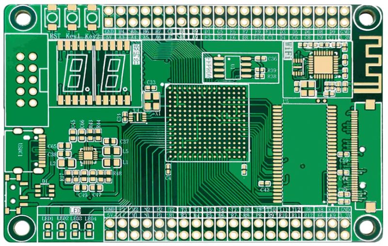
Board 1
Layer: 6 layers
size: 78.05mm*70.37mm
Application: modify hardware accelerator board to FPGA development board
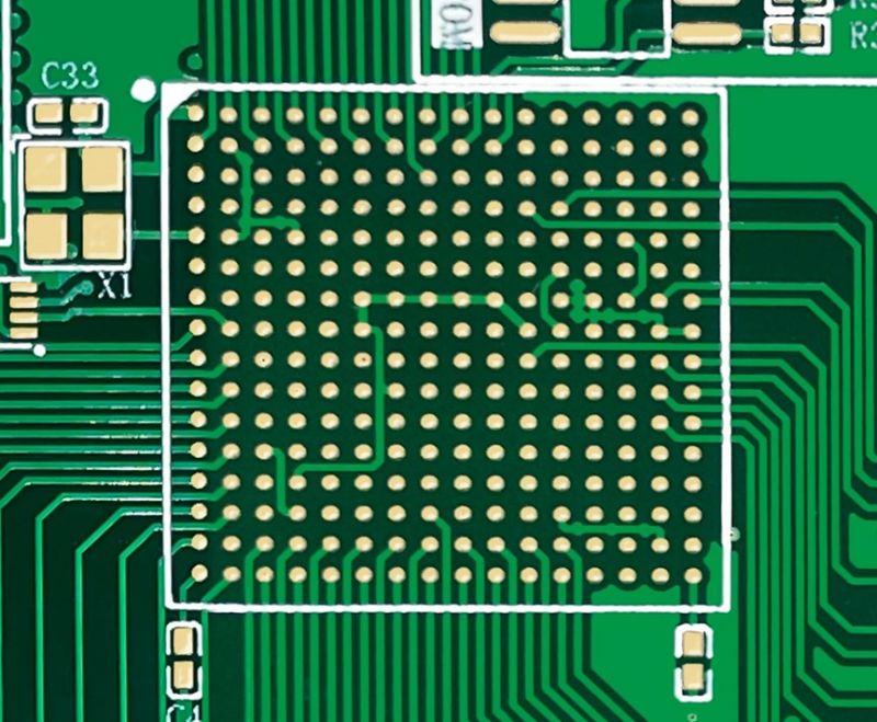
48% of the vias placed on the pads and all BGA packages using vias on the pad (VIA).
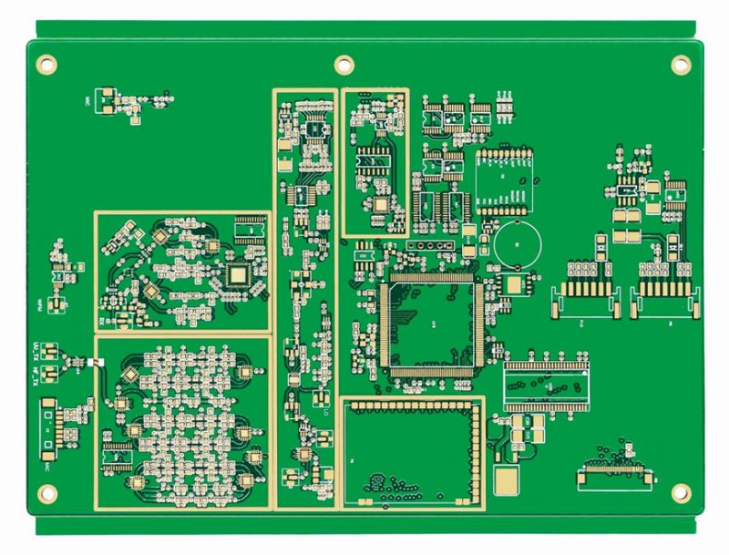
Board 2
Layer: 6 layers
size: 100.05mm*135.05mm
Application: Part of an RF synthesizer for RF signal switching and self-calibration
26% of the vias placed on pads.
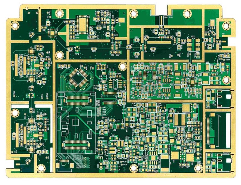
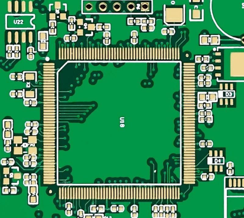
Board 3
Layer: 6 layers
size: 180.07mm *137.14mm
Application: wireless terminal
10% of the vias placed on pads. Via-in-pad on all QFN packages.
Currently, JLCPCB's high-layer PCBs range from 1 to 20 layers. Our factory is actively preparing to expand to even higher layer counts, with plans to extend the options up to 32 layers in the near future.
JLCPCB Coupon Tips You May Need
1. If you are a new user, register on the JLCPCB website to receive up to $54 off coupons covering PCB, PCBA, and 3D printing:
2. JLCPCB automatically sends SMT coupons worth up to $24 to all users every month.
3. Regularly check the JLCPCB Coupon Center for surprise discounts.
JLCPCB is dedicated to accelerating tech innovation. Established in 2006, with over 17 years of continuous improvement, JLC covers every aspect from PCB production and component sourcing to PCB assembly and enclosure fabrication, empowering customers with efficient hardware development and iteration, even with a simple workbench. JLC provides global engineers with rapid and quality deliverables at a favorable budget, accelerating innovation for a world that embraces the wonders of technology.
One-stop Rapid Electronic & Mechatronic Manufacturing
Easy EDA > PCB Prototyping/Small Batch Production > PCB Mass Production > LCSC > Laser Stencil > PCB Assembly > 3D Printing > CNC Machining > FA Mechatronic Parts
[ADVERTISING COLLABORATION]
*JLCPCB also offers a special price of $2 for 1-8 layer FR-4 PCBs (50mm*50mm, 5 pieces) to alleviate the cost burden during project development, enabling innovative ideas to flourish under more favorable conditions. To save more, sign up on JLCPCB official website and get up to $54 off register coupons.
How to Experience Monthly Free 6-8 Layer PCB Prototyping
To enjoy the once-a-month free prototyping, your PCB order needs to meet the following criteria:
• Layer: 6 or 8 layer
• Size: Within 50mm*50mm
• Quantity: 5 pieces
• PCB Specifications: Default settings
To start, you will need to visit the JLCPCB Coupon Center and claim a $2 coupon for 6-8 layer PCBs. Each month, we release one such coupon in the Coupon Center. Remember to claim it before placing your order.
Next, upload the Gerber file that meets the requirements for free prototyping to the quotation page.
Once uploaded successfully, the pricing section on the right side will display the $2 special price for your order. Click "Save to cart" to proceed to the shopping cart.
Click "Secure Checkout" in the cart, then fill in the shipping address and select the appropriate shipping method. If you prefer to pay the bill directly, then click "Continue" to proceed to the payment step.
During payment, apply the $2 coupon you claimed for 6-8 layer PCBs to avail of the discount. You will see that the product cost has been deducted. (In this case, the total price is deducted from $4.17 to only $1.89) Congratulations! You have successfully secured an opportunity for free 6-8 layer PCB prototyping.
Please note that if you select parameters outside the special offer range, such as choosing a panel as the delivery format, a soldermask color other than green, a thicker outer/inner copper weight than the default setting, or if your PCB size exceeds the 50mm*50mm limit for the special offer and you need more than 5 pieces, regular charges will apply.
However, even if your order doesn't qualify for the special offer, rest assured that our regular prices are still favorable. We have made some additional discounts for high-layer PCBs:
• No longer additional charges for via-in-pad for 6-20 layer PCBs.
• For 6-layer PCBs within 10cm*10cm (5pcs) and within 5cm*5cm (10pcs), the price has been reduced from about $85 to $60-63, and the engineering fee adjusted from over $100 to $60 (board thickness within 2.0, 2.0 not included).
JLCPCB High Layer High Quality
With such a discount, can the quality of PCBs be maintained as always? The answer is "Yes"!
At JLCPCB, we deliver cost-effective PCB manufacturing solutions without compromising on performance, durability, and reliability. Backed by our 5 intelligent production bases, we continuously strive for improvement. Through continuous efforts, we've optimized processes, enhanced PCB production layouts, and implemented a comprehensive automated intelligent management system. These initiatives have yielded promising outcomes, also for 6-8 layer PCBs production. Additionally, as our production volume keeps expanding, we can significantly reduce costs because of the large-scale effect on production, allowing us to pass on the savings to every customer. At JLCPCB, we aim to share our years of PCB manufacturing achievements with engineers and makers, giving them a competitive edge by leveraging our production advantages.
JLC's Commitment to PCB Manufacturing
• JLCPCB guarantees full-film PCB manufacturing, without resorting to negative film.
• Via-checking with four-wire low resistance is ensured for all boards.
• High-precision LDI is employed on multi-layer boards(including 4-layer PCBs), for a stable and reliable solder mask bridge.
Before delivering the PCBs to customers, we conduct at least three quality checks:
• Automated Optical Inspection (AOI)
• Flying Probe Testing
• Final Quality Checking piece by piece before shipping
A Peek of JLCPCB multi-layer PCBs with ENIG & via-in-pad
Board 1
Layer: 6 layers
size: 78.05mm*70.37mm
Application: modify hardware accelerator board to FPGA development board
48% of the vias placed on the pads and all BGA packages using vias on the pad (VIA).
Board 2
Layer: 6 layers
size: 100.05mm*135.05mm
Application: Part of an RF synthesizer for RF signal switching and self-calibration
26% of the vias placed on pads.
Board 3
Layer: 6 layers
size: 180.07mm *137.14mm
Application: wireless terminal
10% of the vias placed on pads. Via-in-pad on all QFN packages.
Currently, JLCPCB's high-layer PCBs range from 1 to 20 layers. Our factory is actively preparing to expand to even higher layer counts, with plans to extend the options up to 32 layers in the near future.
JLCPCB Coupon Tips You May Need
1. If you are a new user, register on the JLCPCB website to receive up to $54 off coupons covering PCB, PCBA, and 3D printing:
2. JLCPCB automatically sends SMT coupons worth up to $24 to all users every month.
3. Regularly check the JLCPCB Coupon Center for surprise discounts.
JLCPCB: accelerating your innovation
JLCPCB is dedicated to accelerating tech innovation. Established in 2006, with over 17 years of continuous improvement, JLC covers every aspect from PCB production and component sourcing to PCB assembly and enclosure fabrication, empowering customers with efficient hardware development and iteration, even with a simple workbench. JLC provides global engineers with rapid and quality deliverables at a favorable budget, accelerating innovation for a world that embraces the wonders of technology.
One-stop Rapid Electronic & Mechatronic Manufacturing
Easy EDA > PCB Prototyping/Small Batch Production > PCB Mass Production > LCSC > Laser Stencil > PCB Assembly > 3D Printing > CNC Machining > FA Mechatronic Parts
[ADVERTISING COLLABORATION]