1.Overview
The PIC18F97J60 (Link)family represents a new generation of low-voltage devices within Microchip's portfolio. It combines the traditional strength of PIC18 microcontrollers - high computational performance and a comprehensive feature set - with a highly competitive price point. This makes it an ideal choice for numerous high-performance applications where cost is a crucial factor.

2.Core Features
2.1 Oscillator options and features
All devices in the PIC18F97J60 family offer five distinct oscillator options, providing users with diverse choices for application hardware development:
1.Two Crystal modes, suitable for crystals or ceramic resonators.
2.Two External Clock modes, with an option for a divide-by-4 clock output.
3.A Phase Lock Loop (PLL) frequency multiplier available in external oscillator modes, enabling clock speeds up to 41.667 MHz.
4.An internal RC oscillator with a fixed 31 kHz output, offering an extremely low-power option for timing-insensitive applications.
The internal oscillator block serves as a stable reference source, endowing the family with additional features for reliable operation:
1.Fail-Safe Clock Monitor: Continuously monitors the main clock source against a reference signal from the internal oscillator. In case of clock failure, the controller switches to the internal oscillator for continued low-speed operation or a safe shutdown.
2. Two-Speed Start-up: Allows the internal oscillator to act as the clock source during Power-on Reset or wake-up from Sleep mode until the primary clock source becomes available.

2.1 Expanded memory
The PIC18F97J60 family offers ample space for application code, ranging from 64 Kbytes to 128 Kbytes of code space. The Flash cells for program memory are rated for 100 erase/write cycles, with data retention estimated to exceed 20 years without refresh. Additionally, it provides 3808 bytes of data RAM for dynamic application data.
2.3 External memory bus
In the rare case where 128 Kbytes of memory is insufficient for an application, the 100-pin members of the PIC18F97J60 family implement an External Memory Bus (EMB). This enables the controller's internal program counter to address up to 2 Mbytes of memory space, a level of data access not common among 8-bit devices. It allows for various memory options, such as combining on-chip and external memory up to the 2-Mbyte limit, using external Flash memory for reprogrammable code or large data tables, and using external RAM for storing large amounts of variable data.
When you need extra memory flexibility, the PIC18F97J60 family's EMB has you covered. For more storage solutions and technical advice, turn to Unikeyic (Link) component platform, available for purchase online.
2.4 Extended instruction set
The PIC18F97J60 family offers ample space for application code, ranging from 64 Kbytes to 128 Kbytes of code space. The Flash cells for program memory are rated for 100 erase/write cycles, with data retention estimated to exceed 20 years without refresh. Additionally, it provides 3808 bytes of data RAM for dynamic application data.
2.5 Easy migration
Regardless of the memory size, all devices share the same rich set of peripherals, allowing for a smooth migration path as applications grow and evolve.
3.Other Special Features
• Communications: The family incorporates multiple serial communication peripherals, including up to two independent Enhanced USARTs and two Master SSP modules capable of SPI and I2C™ (Master and Slave) modes. Additionally, one general-purpose I/O port can be reconfigured as an 8-bit Parallel Slave Port for direct processor-to-processor communication.
• CCP Modules: All devices feature two Capture/Compare/PWM (CCP) modules and three Enhanced CCP (ECCP) modules, maximizing flexibility in control applications. Up to four different time bases can be used for simultaneous operations. Each ECCP module offers up to four PWM outputs, totaling twelve PWMs. The ECCP modules also include beneficial features like polarity selection, programmable dead time, auto-shutdown and restart, and Half-Bridge and Full-Bridge Output modes.
• 10-Bit A/D Converter: This module allows for programmable acquisition time, enabling channel selection and conversion initiation without waiting for a sampling period, reducing code overhead.
• Extended Watchdog Timer (WDT): The enhanced version features a 16-bit prescaler, providing an extended time-out range.
4.Interpreting the Naming Convention of PIC18F67J60T-I/PT Model
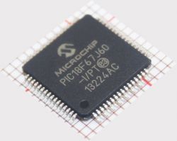
The product code PIC18F67J60T-I/PT has specific meanings. "PIC" indicates the product line. "18F" denotes its membership in the high-end series. "67" refers to the memory capacity. "J60" represents distinctions in operational parameters. The presence or absence of "T" indicates a packaging difference. "I" signifies an industrial-grade temperature range from -45°C to 85°C, and "PT" stands for a thin quad flat package with four leads on each side.
Microchip offers eight different series, with PIC10, 12, 16, and 18 being 8-bit microcontrollers, PIC24, 30, and 33 as 16-bit microcontrollers, and PIC32 as a 32-bit microcontroller. Higher bit numbers generally imply increased computational and storage capacity, processing speed, and feature expandability. The choice depends on the application requirements and budget.
The PIC18F97J60 (Link)family represents a new generation of low-voltage devices within Microchip's portfolio. It combines the traditional strength of PIC18 microcontrollers - high computational performance and a comprehensive feature set - with a highly competitive price point. This makes it an ideal choice for numerous high-performance applications where cost is a crucial factor.

2.Core Features
2.1 Oscillator options and features
All devices in the PIC18F97J60 family offer five distinct oscillator options, providing users with diverse choices for application hardware development:
1.Two Crystal modes, suitable for crystals or ceramic resonators.
2.Two External Clock modes, with an option for a divide-by-4 clock output.
3.A Phase Lock Loop (PLL) frequency multiplier available in external oscillator modes, enabling clock speeds up to 41.667 MHz.
4.An internal RC oscillator with a fixed 31 kHz output, offering an extremely low-power option for timing-insensitive applications.
The internal oscillator block serves as a stable reference source, endowing the family with additional features for reliable operation:
1.Fail-Safe Clock Monitor: Continuously monitors the main clock source against a reference signal from the internal oscillator. In case of clock failure, the controller switches to the internal oscillator for continued low-speed operation or a safe shutdown.
2. Two-Speed Start-up: Allows the internal oscillator to act as the clock source during Power-on Reset or wake-up from Sleep mode until the primary clock source becomes available.

2.1 Expanded memory
The PIC18F97J60 family offers ample space for application code, ranging from 64 Kbytes to 128 Kbytes of code space. The Flash cells for program memory are rated for 100 erase/write cycles, with data retention estimated to exceed 20 years without refresh. Additionally, it provides 3808 bytes of data RAM for dynamic application data.
2.3 External memory bus
In the rare case where 128 Kbytes of memory is insufficient for an application, the 100-pin members of the PIC18F97J60 family implement an External Memory Bus (EMB). This enables the controller's internal program counter to address up to 2 Mbytes of memory space, a level of data access not common among 8-bit devices. It allows for various memory options, such as combining on-chip and external memory up to the 2-Mbyte limit, using external Flash memory for reprogrammable code or large data tables, and using external RAM for storing large amounts of variable data.
When you need extra memory flexibility, the PIC18F97J60 family's EMB has you covered. For more storage solutions and technical advice, turn to Unikeyic (Link) component platform, available for purchase online.
2.4 Extended instruction set
The PIC18F97J60 family offers ample space for application code, ranging from 64 Kbytes to 128 Kbytes of code space. The Flash cells for program memory are rated for 100 erase/write cycles, with data retention estimated to exceed 20 years without refresh. Additionally, it provides 3808 bytes of data RAM for dynamic application data.
2.5 Easy migration
Regardless of the memory size, all devices share the same rich set of peripherals, allowing for a smooth migration path as applications grow and evolve.
3.Other Special Features
• Communications: The family incorporates multiple serial communication peripherals, including up to two independent Enhanced USARTs and two Master SSP modules capable of SPI and I2C™ (Master and Slave) modes. Additionally, one general-purpose I/O port can be reconfigured as an 8-bit Parallel Slave Port for direct processor-to-processor communication.
• CCP Modules: All devices feature two Capture/Compare/PWM (CCP) modules and three Enhanced CCP (ECCP) modules, maximizing flexibility in control applications. Up to four different time bases can be used for simultaneous operations. Each ECCP module offers up to four PWM outputs, totaling twelve PWMs. The ECCP modules also include beneficial features like polarity selection, programmable dead time, auto-shutdown and restart, and Half-Bridge and Full-Bridge Output modes.
• 10-Bit A/D Converter: This module allows for programmable acquisition time, enabling channel selection and conversion initiation without waiting for a sampling period, reducing code overhead.
• Extended Watchdog Timer (WDT): The enhanced version features a 16-bit prescaler, providing an extended time-out range.
4.Interpreting the Naming Convention of PIC18F67J60T-I/PT Model
The product code PIC18F67J60T-I/PT has specific meanings. "PIC" indicates the product line. "18F" denotes its membership in the high-end series. "67" refers to the memory capacity. "J60" represents distinctions in operational parameters. The presence or absence of "T" indicates a packaging difference. "I" signifies an industrial-grade temperature range from -45°C to 85°C, and "PT" stands for a thin quad flat package with four leads on each side.
Microchip offers eight different series, with PIC10, 12, 16, and 18 being 8-bit microcontrollers, PIC24, 30, and 33 as 16-bit microcontrollers, and PIC32 as a 32-bit microcontroller. Higher bit numbers generally imply increased computational and storage capacity, processing speed, and feature expandability. The choice depends on the application requirements and budget.


