Upgrade Your PCB Design Workflow with JLCPCB’s Layout Services and One-Stop Manufacturing
JLCPCB: Professional PCB Layout Services Backed by Full One-Stop Manufacturing
Introduction
The progress of modern electronics has been a nightmare of disrupted workflow for engineers. After creating an advanced circuit, you transfer the diagrams to one supplier for PCB layout design, send the Gerber files to a different supplier for fabrication, and then deal with a third supplier for buying components. Every time the design is passed on, it leads to miscommunication and a delay in time.
JLCPCB has done away with these friction points. We, as a truly integrated One-Stop Electronic Manufacturing Platform, connect the idea with the hardware. It does not matter if you are going to develop a prototype for an IoT device or design printed circuit board that operates at high speed; our ecosystem allows you to transition smoothly from design files to the product.
What is JLCPCB?
JLCPCB stands as one of the largest PCB prototype manufacturers, serving over 6.220,000 customers globally since 2006. But calling it simply a "PCB manufacturer" understates its comprehensive service portfolio. JLCPCB provides a true turnkey PCBA workflow through integrated PCB fabrication, in-stock parts sourcing, and SMT assembly.
By consolidating these critical stages, JLCPCB operates as a complete one-stop electronic manufacturing platform:
Core Service Ecosystem:
● PCB Fabrication: From simple 2-layer prototypes to complex 20-layer HDI boards, specialized aluminum-backed thermal designs, and high-quality Flex PCBs. Advanced capabilities include laser direct imaging (LDI) for 3.5 mil trace/space precision.
● PCB Assembly: The JLCPCB SMT service maintains an inventory exceeding 350,000 component types with 24-hour turnaround capabilities.
● Professional JLCPCB Layout Service: JLCPCB offers a layout service where certified engineers turn your schematics into manufacturable designs.
● Ancillary Manufacturing: Complementary services include laser-cut stencils, 3D printing for enclosures, CNC machining, and customized Flexible Heaters.
| Service Category | Key Capabilities | Turnaround Time |
| PCB Fabrication | 1-32 layers, HDI, Flex PCB | 24-48 hours |
| SMT Assembly | 2 - 80000 pcs, 0201 - BGA | 24 hours |
| Design Layout | Schematic to Gerber conversion | 3-5 days |
| Stencil Manufacturing | Laser/electropolish finish | 24 hours |
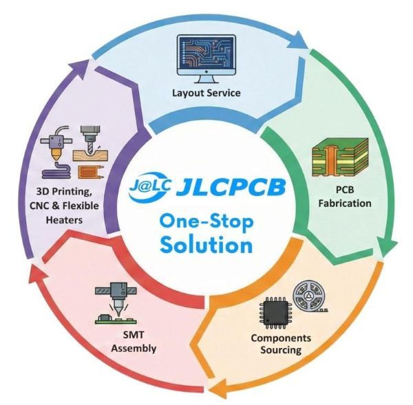
JLCPCB integrated electronics manufacturing ecosystem infographic
JLCPCB Layout Service - From Design to Manufacturing, Seamlessly
What Is PCB Layout?
PCB layout represents the physical realization of schematic circuitry onto copper-clad laminate boards. While schematics define logical connectivity, PCB layout design work determines the precise geometric implementation: where components physically reside, how traces route between pins, and how power is distributed across planes.
This distinction matters profoundly. A flawless schematic can fail catastrophically with poor layout execution. Consider a high-speed USB 3.0 interface: the schematic simply shows differential pair connections. The design printed circuit implementation requires maintaining 90-ohm controlled impedance, keeping pair traces within 5 mils length matching, and positioning decoupling capacitors within 10mm of IC power pins.
Modern Layout Complexity:
● High-Speed Digital: DDR4 memory running at 3200 MT/s typically requires length matching within ±5 to ±50 mils, depending on the signal group.
● RF Circuits: Wireless designs operating at frequencies above 2.4 GHz necessitate coplanar waveguide shapes and dielectric materials with specific properties.
● Power Integrity: Today's CPUs, consuming more than 50 amps, require power supply networks whose resistance is less than 1 milliohm.
● Miniaturization: The use of 0201-size electronic parts and 0.4mm pitch ball grid arrays presents manufacturing problems that can be solved only through an expert PCB layout design.
| Aspect | Schematic Design | PCB Layout Design |
| Primary Focus | Logical connectivity | Physical geometry |
| Key Deliverable | Net list, BOM | Gerber files, drill data |
| Main Concerns | Circuit functionality | Signal integrity, EMI, DFM |
Fundamental differences between schematic and PCB layout design
Professional PCB Layout Design Workflow
Step 1: Prepare the Schematic and Component List
A thorough preparation is necessary for professional layout: netlist validation, component footprints checking (according to IPC-7351), stack-up definition (layer count, materials, copper weights), and rules for design creation. Minimum trace width for signals normally starts at 4 mils, and for power traces carrying >1A current, it is from 8-15 mils.
Step 2: Place Components Logically
Component positioning is responsible for 80% of the routing success. Among the main strategies, JLCPCB can mention:
● Functional Zoning: Power supplies must be separated from sensitive analog circuits, and high-speed digital circuits must be isolated from RF sections.
● Thermal Management: Components that are dissipating more than 0.5W should have a clearance of more than 5mm and thermal vias to the ground planes.
● Critical Signals: Clock distribution and reset lines need short, direct routing.
● Decoupling Proximity: High-frequency capacitors must sit within 10mm of IC power pins.
Step 3: Route the PCB Traces
Routing necessitates an advanced comprehension of signal behavior:
● Differential Pairs: USB requires 90Ω impedance with <5 mil intra-pair skew. Use the 3W spacing rule for proper coupling.
● High-Speed Signals: DDR4 needs ±500 mil matching over byte lanes with via count minimization.
● Power Distribution: Determine the trace width based on current - 1OZ copper 10 mil trace can carry ~1A with 10°C rise.
Why Choose JLCPCB Layout?
The design department and manufacturing process are interlinked securely with our layout service, which is the one that completes the circuit between design and production.
● Integrated With Manufacturing: JLCPCB leverages EasyEDA and extensive production experience to ensure seamless integration from design layout to PCB to final production.
● Professional & Experienced Layout Team: JLCPCB senior engineers solves complex signal interference, thermal, and EMC challenges for high-density and high-speed boards.
● Faster Turnaround Time: By applying verified manufacturing guidelines and in-house production data, JLCPCB delivers complex designs more promptly.
● Cost Optimization: JLCPCB optimizes designs to minimize production costs while ensuring high performance, offering special discounts on fabrication and assembly.
JLCPCB Layout Service Workflow
JLCPCB process is transparent, collaborative, and designed for speed.
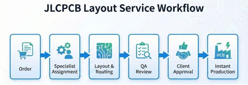
Flowchart depicting the JLCPCB Layout Service workflow from initial design layout PCB request to final manufacturing.
1. Place an Order: Submit your schematics, BOM, and mechanical constraints.
2. Order Review & Payment: Our engineers review your files for completeness and confirm requirements before payment is processed.
3. Allocate Engineers: JLCPCB assigns a specialist suited to your domain (e.g., RF, Power, Digital).
4. Layout Execution: JLCPCB performs the physical design layout PCB work, iterating on placement and routing.
5. Chief Engineer Review: The internal quality assurance checks confirm the integrity of the signal and the compliance with DFM.
6. Client Confirmation: You review 3D renders and Gerber files.
7. Order Completed: Files exported directly to the JLCPCB production queue.
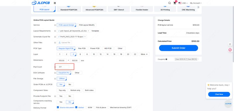
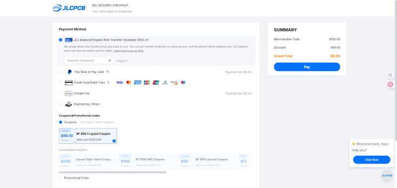
JLCPCB Layout Service Starts from ¥9.9 on Black Friday
JLCPCB pricing system has been restructured to support both engineers and startups. During JLCPCB promotional events, such as Black Friday, it is possible to speed up your PCB layout design process for basic boards at a price as low as ¥9.9. This low entry price not only makes it possible for you to shift daily layout activities to us but also allows you to devote your time to system design and firmware development.
JLCPCB: A Leading PCB Prototyping Company
Although the layout service acts as a connector, the manufacturing capability is still the main strength of our company.
Advanced Manufacturing
JLCPCB have installed state-of-the-art automated production lines using LDI (Laser Direct Imaging) technology for ultra-fine trace definition. This enables JLCPCB to produce boards with 3.5-mil-wide traces that can cope with fine-pitch BGAs without a hitch.
Turnaround
Speed is JLCPCB currency. For standard 2-layer boards, our fabrication time can be as fast as 24 hours. This rapid iteration cycle enables R&D teams to test and debug hardware in days, not weeks.
High Quality & Production Testing
All boards have to pass the AOI (Automated Optical Inspection) and Flying Probe Testing to guarantee electrical continuity. For your assembled boards, the X-ray inspection method is available for you to check BGA soldering quality, making sure that hidden joints are free of defects and that void percentages do not exceed IPC limits.
Price of Prototyping
Economies of scale allow us to offer unbeatably low prices (e.g., $2 for 5 PCBs) without compromising the substrate quality.
JLCPCB SMT
Our JLCPCB SMT service is the logical next step. With over 350,000+ parts in our library, we can assemble your boards immediately after fabrication.
Global Sourcing & Assembler’s Parts Library
The Parts Library of our Assembler directly integrates with the parts library of JLCPCB and with the parts libraries of global distributors. This confirmation makes it impossible that the parts of your printed circuit BOM design will not be genuine, will not be in stock, and will not be ready for assembly, thus reducing the supply chain risks to a large extent.
JLCPCB: Stencil
For clients performing in-house assembly, we provide high-precision laser-cut stainless steel stencils. These ensure accurate solder paste deposition, which is critical for preventing bridges on fine-pitch components.
JLCPCB: Flexible Heater
We support advanced technologies, including Flexible Heaters (FH) and Flex-PCBs. These are increasingly vital for automotive and medical applications where thermal regulation is required within a compact, non-planar form factor.
Best Circuit Board Design Software Online: EasyEDA
A seamless platform requires seamless tools. EasyEDA is a web-based EDA tool tailored for cloud collaboration. It integrates directly with the JLCPCB component library, allowing you to select parts that are "Ready for Assembly" while you draw your schematic. It supports robust design layout PCB features, including auto-routing and direct Gerber generation.
Conclusion
The practice of isolated electronics manufacturing is over. JLCPCB stands as the definitive One-Stop Electronic Manufacturing Platform, empowering engineers to move from a napkin sketch to a finished PCBA faster and more reliably. Whether you need expert assistance with design printed circuit tasks or simply need a fast fabrication house, we have the infrastructure to support you.
Ready to start? Try JLCPCB Today. New customers can sign up for $70 coupons, and our Layout Service starts as low as $9.9!
FAQs
Q1: How much time does a typical layout project take?
For standard projects (e.g., 2-4 layers, moderate complexity), our turnaround is typically 2-4 business days. Simpler design layout PCB tasks can often be completed faster, while complex high-speed designs may require additional time for rigorous signal integrity verification.
Q2: Can beginners use the JLCPCB Layout Service?
Absolutely. Our service is aimed at anyone who wants to convert a schematic to a professional printed circuit design. If you have any doubts about layout rules or stack-ups, our engineers will take you by the hand and walk you through the entire process to deliver a manufacturable product.
Q4: How does JLCPCB ensure DFM compliance?
Being both the layout service and the manufacturer, we directly design according to our factory’s capabilities. In layout time, we do DFM (Design for Manufacturability) checks in real-time to make sure minimum clearances, drill sizes, and solder mask expansion conform to our manufacturing standards, thus ensuring a board that is 100% manufacturable.
Q4: Can I request revisions if I need changes?
Yes. Design is a process that usually requires multiple iterations, and JLCPCB acknowledges that. A review is usually part of our service, where the layout is shown to you, and changes are made according to your requests before JLCPCB finalize the files for production.
[Advertising Partnership with JLCPCB - Jialichuang (HongKong) CO. Ltd.]


