What Is a Semiconductor ?
Semiconductors are materials with conductivities halfway between those of insulators and conductors. Semiconductors can be made of pure elements, like silicon or germanium, or from a blend of substances, like gallium arsenide or cadmium selenide. A doping approach alters the conductivity of the material by adding impurities to pure semiconductors.
Atomic structure
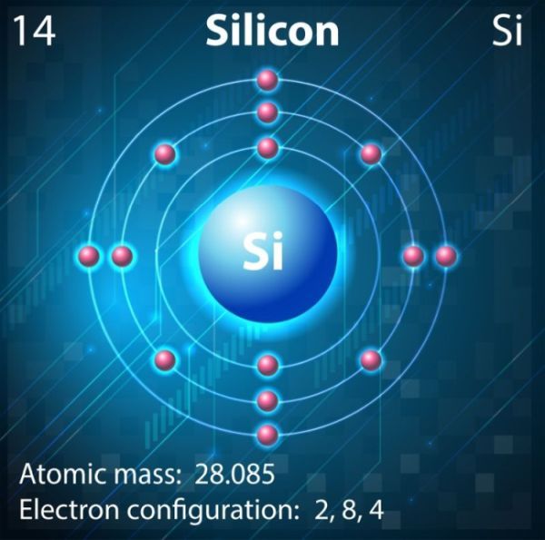
The diagram of the atomic structures of silicon (Si) is shown in Figure 1. With an atomic number of 14, silicon is a common material, since it covers up to 28% of the Earth’s surface.
By observing Figure 1, we can note how silicon has four electrons in its outer ring. These electrons, also known as valence electrons, can in some cases bond with the valence electrons of another atom. When this occurs, we have a covalent bond, which results in a lattice crystalline structure.
In its pure form, silicon is a good insulator, meaning it will not conduct electricity. However, by adding some impurities to a pure silicon structure, we can modify the conduction characteristics of this semiconductor.
Therefore, doping is the addition of impurities to a pure semiconductor material. While a pure semiconductor is intrinsic, doping produces an extrinsic semiconductor, indicating that the substance isn't entirely pure.
The most common types of impurities are trivalent (three valence electrons) and pentavalent (five valence electrons) impurities. Examples of trivalent are boron and gallium, while examples of pentavalent are arsenic and antimony.
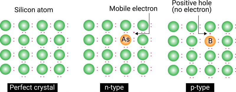
Suppose pure silicon semiconductor is doped with arsenic (pentavalent). Four valence electrons of arsenic will form a covalent bond with the four valence electrons of silicon, while one electron from the arsenic remains free. In this case, we say that arsenic donated a free electron to the structure.
More generally, all pentavalent impurities are called donor impurities because they donate free electrons. In the resulting structure (see Figure 2), electricity is conducted by electrons and the crystal is called an N-type crystal.
Vice versa, since trivalent impurity can use only three electrons to form a covalent bond, one more electron will be needed to complete the lattice structure. In this case, a hole will remain in the place of the missing electron. Since this hole can accept an electron, trivalent impurity is called an acceptor impurity. In the resulting structure, electricity is conducted by positive holes and the crystal is called a P-type crystal.
The P-N junction
In a P-type semiconductor, the group III element of the periodic table is added as the dopant element, while in the N-type the group V element is the dopant element. In a P-type semiconductor, the majority carriers are holes, and the minority carriers are electrons.
The P-N junction is an interface composed of two differently doped semiconductor types. In the P zone, there are trivalent doping elements which therefore have one more gap (more positive charge) than the semiconductor of which the junction is formed, while in the N zone there are pentavalent doping elements, and therefore with an electron more (more negative charge).
The term junction refers to the region where the two types of doping (P and N) join. Therefore, if we put the the P-type and the N-type layers close together, in the junction an emptying zone is created as the holes in the P zone tend to approach the N layer, and the electrons in the N zone tend to move towards the P zone. The emptying area therefore appears to be devoid of charges as the neighboring ones have neutralized each other.
In the junction, therefore, an electric field is created that goes from right to left (towards from plus to minus) and a difference in potential delta V with the opposite direction to the electric field.
The P zone is also called the acceptor zone, as it accepts electrons in its zone. The N zone is also called the donor zone, as it donates electrons to the P zone.
The diode
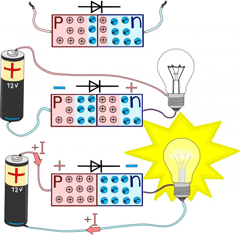
Now, suppose we electronically connect a PN junction with a battery as shown in Figure 3. If we connect the P area of the junction with the positive pole of the battery and the N area with the negative pole of the battery, we say that we have connected the PN junction in direct polarization.
In this case, the PN junction will be crossed by a current as the negative charges of the N area are attracted to the positive pole of the battery, and after having overcome the potential difference of the junction they reach the positive pole of the battery. At the same time, the holes are neutralized by the electrons.
If, on the other hand, we connect the PN junction in reverse polarization, just connect the P area with the negative pole of the battery and the N area with the positive pole of the battery. In this case, no current will circulate inside the junction as the emptying area will widen, not allowing any charge to pass through it.
The diode is a passive, non-linear electronic component with two terminals, whose function is to be crossed by the current only in one direction, the direct polarization, and not to be crossed by the current when polarization is inverse.


