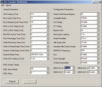
For many, mysterious timings are still black magic. There is a lot of talk and writing about them, but you don't know what they really are and what they are supposed to serve. I will try to help you understand the essence of the timings themselves, their recording and I will explain how to set them in accordance with the manufacturer's data.
I will focus only on DDR memory, which is still quite popular, and on DDR2. Due to the lack of my knowledge about them, DDR3 will not be taken into account. SDRAM will also not find its place here due to the fact that it is almost forgotten .
.
Timings
The simplest way to say is that these are the settings of our memory parameters. These are the delays of successive functions performed by the module with respect to the timing clock.
The basic notation and the most common to represent timings is as follows:
ABCDE xxxMHz.
Now in turn:
A - CAS Latency (CL)
B - RAS-to-CAS Delay (tRCD)
C - RAS Precharge Time (tRP)
D - Cycle Time (tRAS)
E - Command Rate (CR)
xxxMHz - this is the memory clock speed.
tCAS
CAS Latency (CL) is perhaps the most common delay setting. It specifies the number of bus clock cycles that elapsed from the CPU issuing the column select activation command to the time the data is transferred to the buffer in the memory controller. It has quite a big impact on performance, especially for players of the 3DMark and Quake III religions. In the case of DDR modules, this factor is usually 2.5, and it can be set in the range from 2.0 to 3.0 (although on some boards it is possible to set CL1.5 and CL1), in the case of SDRs we can usually set CL2 or CL3.
tRCD
The RCD time (RAS to CAS delay) determines how many clock ticks it takes after executing the CAS command and thus locating the needed column to perform RAS loading. At low settings, it gives a small but visible 'kick' to the system.
trass
The RAS (Row Address Strobe) time specifies the number of cycles required to execute an activation command for one of the memory banks before loading a row address can be performed. By itself, it doesn't give you too much of a performance gain with sharper settings.
tRP
The RP (RAS Precharge) parameter is the number of clock ticks needed to restore the data to its original position, close the bank, or the number of cycles required to paging the memory before executing the next bank activation command. It also doesn't have much impact on performance.
It looks like this for my DDR2:
4-4-4-12-1T 400MHz (DDR2 800).
CL - 4
tRCD -4
tRp - 4
tRAS -12
CR - 1
clocked 400MHz - this is the actual clock of the module. The most common way of specifying the memory timing is the effective timing, i.e. as given in parentheses.
I will not elaborate and explain why this is the case and where the actual and effective timing records come from. Please use Google or Wikipedia and read for yourself. The beginning of the reading will be the definition of DDR RAM memory and their principle of operation and difference from SDRAM.
How do I find out what timings to set for my memories?
You can read on the packaging:

Sticker located on the memory module:
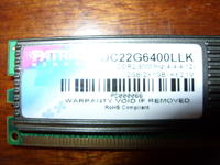
or download the CPU-Z program from the Internet and in the SPD tab, read the settings saved by the manufacturer in the SPD system used for auto-configuration of memory via the BIOS.
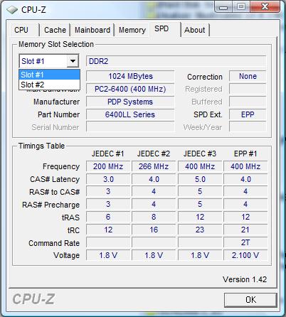
You already know what the timings for your memory should be according to their timing, so we're taking a trip to the BIOS.
Manual configuration of timings
This is more or less the bios page responsible for configuring memory timings:
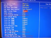
The underlined options are the basic timings.
Depending on the motherboard manufacturer, the name of this page may be:
DRAM timings
DDR timings
RAM configuration
Memory timings
e.t.c...
By default, in the bios, the Auto option will most likely be set, i.e. the bios will read the settings from the SPD of the modules and set what and how. Unfortunately, it often does not work well and causes worse delays.
Depending on the BIOS, the timing list will be visible but inactive, or it will appear after switching the configuration to Manual.
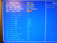
Find ONLY the options responsible for the basic timings and set them according to the manufacturer's recommendations. As you can see in the screen above, there are definitely more options that beginners should not change. Most of them are minor timings responsible for the stability of the systems operation and having a negligible impact on performance. Changing these timings basically makes sense only with a very high memory overclock and you change them to increase stability.
If you have set what I indicated in the picture, you can save the settings and start the computer.
You should see your CPU-Z changed on the Memory page.
That's it for beginners. Overclockers I invite you to read on .
.
What is the most effective setting on my platform?
AMD
For the platform socket A the first and most important setting is the SYNCHRONOUS mode of the FSB memory, i.e. a 1: 1 divider.
Asynchronous mode has a significant impact on performance degradation.
The next step is to obtain the highest FSB clock speed and thus DRAM with the sharpest possible timings.
CAS Latency (CL) - 2, 2.5, 3 - 2 is a dream and requires very good memories. Some memories won't work with CL other than 3 on socket A.
RAS to CAS Delay (tRCD) - 2, 3, 4 - 4 try to avoid at all costs is the worst setting. your goal is 2.
RAS Precharge (tRP) - as above 2, 3, 4 - and as above also aim for 2.
Cycle Time (tRAS) - it's not easy here anymore. Initially and in the simplest way, it can be assumed that for efficient work we shouldhave tRAS = CL + tRCD + tRP unfortunately this method almost always goes against nForce motherboards. With 2.5-3-3 timings, the calculated tRAS would be 8, and the most efficient was 11. In the same configuration on nForce4, the most effective tRAS was 6. In general, you can only rely on the calculation only nForce owners should try a bit of testing and find the best tRAS for themselves .
Command Rate (CR) - 1T / 2T
There is also the Dual Channel mode (what it is and how it works, I refer to Wikipedia), which on this platform has little impact on performance.
AMD64 socket 754
You set all timings as for socketA. You want the sharpest settings and highest timing possible. It often makes no sense to loosen the timings for better timing. Know that:
2-2-2-5-1T 240MHz is as efficient as 2.5-3-3-6-2T at 270MHz.
By following sharper timings and a lower clock, you save the temperature memories.
I pay special attention to the Command Rate. On p. 754 it has a special meaning.
1T has a huge impact on memory performance. From my personal tests, the throughput can increase by 400-500MB / s. Unfortunately, nothing is for free and this is reflected in the stability of the systems. The 1T starts to bite with high clock speeds (about 10-20% more than the nominal one and problems begin). For example, 1T worked perfectly at 200MHz but at 220MHz the memtest already showed errors, with the other timings set the same.
2T, as shown above, significantly increases memory stability at the expense of performance.
Dual-Channel on socket 754 DOES NOT EXIST!
AMD64 socket939
Here, for the first time, the basis for efficient memory operation is the efficient Dual Channel mode !!
In the early days of the platform, it operated with DDR memory. Later p.939 boards with support for the newer DDR2 were made.
For DDR the case is like for p.754 only the critical requirement is Dual Channel operation. 2x512MB in dual works more efficiently than 3x512MB in single !!
If you have p.939 on DDR memory then you are aiming for the lowest timings and high clock speeds as in p.754.
If you already have DDR2 ...
Here are the new values for timings:
CL - 4, 5, 6
tRCD - 4, 5, 6
tRP - 4, 5, 6
tRAS - 10-18
CR - 1T / 2T
The typical and most common ones are 5-5-5-15 and 4-4-4-12 (memories designed for CL4 are slightly more expensive than CL5.) As you will soon notice tRAS = tRP + tRCD + CL. The memory of the CL6 is avoided like fire.
the setting of the CR 1T / 2T is by the wayside. In DDR2 1T memory, it does not have such a drastic impact on performance. Yes, it still slightly increases the efficiency, but it is not enough that instead of 5-5-5-15-1T, it is definitely better to try 4-4-4-12-2T. As you can guess, the CR has no such impact on performance, and thus the loss of stability is smaller. With DDR2, the 1T / 2T setting is of marginal importance for stability. Often in forum discussions there are disputes about the stability of the CR setting with DDR2. I am ahead of these disputes - it has no significant impact on memory stability and switching to 2T will not give you a chance for higher clock speeds or sharper timings as it was in the case of DDR on p. 754.
AMD64 s.AM2 (p. 940)
There is nothing to dwell on here either. Memory configuration is the same as for p. 939 with DDR2 memories. The same rules apply.
Important note
Very often there are topics asking for help in memory configuration where the basic error is DDR2 in Single mode. To run a memory set prepared to work in Dual-Channel (the so-called Dual-Channel Kit), you place the modules in the SAME COLOR sockets.
Intel owners, please be patient
Sources:
The definitions of individual timings come from:
PurePC
I will focus only on DDR memory, which is still quite popular, and on DDR2. Due to the lack of my knowledge about them, DDR3 will not be taken into account. SDRAM will also not find its place here due to the fact that it is almost forgotten
Timings
The simplest way to say is that these are the settings of our memory parameters. These are the delays of successive functions performed by the module with respect to the timing clock.
The basic notation and the most common to represent timings is as follows:
ABCDE xxxMHz.
Now in turn:
A - CAS Latency (CL)
B - RAS-to-CAS Delay (tRCD)
C - RAS Precharge Time (tRP)
D - Cycle Time (tRAS)
E - Command Rate (CR)
xxxMHz - this is the memory clock speed.
tCAS
CAS Latency (CL) is perhaps the most common delay setting. It specifies the number of bus clock cycles that elapsed from the CPU issuing the column select activation command to the time the data is transferred to the buffer in the memory controller. It has quite a big impact on performance, especially for players of the 3DMark and Quake III religions. In the case of DDR modules, this factor is usually 2.5, and it can be set in the range from 2.0 to 3.0 (although on some boards it is possible to set CL1.5 and CL1), in the case of SDRs we can usually set CL2 or CL3.
tRCD
The RCD time (RAS to CAS delay) determines how many clock ticks it takes after executing the CAS command and thus locating the needed column to perform RAS loading. At low settings, it gives a small but visible 'kick' to the system.
trass
The RAS (Row Address Strobe) time specifies the number of cycles required to execute an activation command for one of the memory banks before loading a row address can be performed. By itself, it doesn't give you too much of a performance gain with sharper settings.
tRP
The RP (RAS Precharge) parameter is the number of clock ticks needed to restore the data to its original position, close the bank, or the number of cycles required to paging the memory before executing the next bank activation command. It also doesn't have much impact on performance.
It looks like this for my DDR2:
4-4-4-12-1T 400MHz (DDR2 800).
CL - 4
tRCD -4
tRp - 4
tRAS -12
CR - 1
clocked 400MHz - this is the actual clock of the module. The most common way of specifying the memory timing is the effective timing, i.e. as given in parentheses.
I will not elaborate and explain why this is the case and where the actual and effective timing records come from. Please use Google or Wikipedia and read for yourself. The beginning of the reading will be the definition of DDR RAM memory and their principle of operation and difference from SDRAM.
How do I find out what timings to set for my memories?
You can read on the packaging:

Sticker located on the memory module:

or download the CPU-Z program from the Internet and in the SPD tab, read the settings saved by the manufacturer in the SPD system used for auto-configuration of memory via the BIOS.

You already know what the timings for your memory should be according to their timing, so we're taking a trip to the BIOS.
Manual configuration of timings
This is more or less the bios page responsible for configuring memory timings:

The underlined options are the basic timings.
Depending on the motherboard manufacturer, the name of this page may be:
DRAM timings
DDR timings
RAM configuration
Memory timings
e.t.c...
By default, in the bios, the Auto option will most likely be set, i.e. the bios will read the settings from the SPD of the modules and set what and how. Unfortunately, it often does not work well and causes worse delays.
Depending on the BIOS, the timing list will be visible but inactive, or it will appear after switching the configuration to Manual.

Find ONLY the options responsible for the basic timings and set them according to the manufacturer's recommendations. As you can see in the screen above, there are definitely more options that beginners should not change. Most of them are minor timings responsible for the stability of the systems operation and having a negligible impact on performance. Changing these timings basically makes sense only with a very high memory overclock and you change them to increase stability.
If you have set what I indicated in the picture, you can save the settings and start the computer.
You should see your CPU-Z changed on the Memory page.
That's it for beginners. Overclockers I invite you to read on
What is the most effective setting on my platform?
AMD
For the platform socket A the first and most important setting is the SYNCHRONOUS mode of the FSB memory, i.e. a 1: 1 divider.
Asynchronous mode has a significant impact on performance degradation.
The next step is to obtain the highest FSB clock speed and thus DRAM with the sharpest possible timings.
CAS Latency (CL) - 2, 2.5, 3 - 2 is a dream and requires very good memories. Some memories won't work with CL other than 3 on socket A.
RAS to CAS Delay (tRCD) - 2, 3, 4 - 4 try to avoid at all costs is the worst setting. your goal is 2.
RAS Precharge (tRP) - as above 2, 3, 4 - and as above also aim for 2.
Cycle Time (tRAS) - it's not easy here anymore. Initially and in the simplest way, it can be assumed that for efficient work we shouldhave tRAS = CL + tRCD + tRP unfortunately this method almost always goes against nForce motherboards. With 2.5-3-3 timings, the calculated tRAS would be 8, and the most efficient was 11. In the same configuration on nForce4, the most effective tRAS was 6. In general, you can only rely on the calculation only nForce owners should try a bit of testing and find the best tRAS for themselves .
Command Rate (CR) - 1T / 2T
There is also the Dual Channel mode (what it is and how it works, I refer to Wikipedia), which on this platform has little impact on performance.
AMD64 socket 754
You set all timings as for socketA. You want the sharpest settings and highest timing possible. It often makes no sense to loosen the timings for better timing. Know that:
2-2-2-5-1T 240MHz is as efficient as 2.5-3-3-6-2T at 270MHz.
By following sharper timings and a lower clock, you save the temperature memories.
I pay special attention to the Command Rate. On p. 754 it has a special meaning.
1T has a huge impact on memory performance. From my personal tests, the throughput can increase by 400-500MB / s. Unfortunately, nothing is for free and this is reflected in the stability of the systems. The 1T starts to bite with high clock speeds (about 10-20% more than the nominal one and problems begin). For example, 1T worked perfectly at 200MHz but at 220MHz the memtest already showed errors, with the other timings set the same.
2T, as shown above, significantly increases memory stability at the expense of performance.
Dual-Channel on socket 754 DOES NOT EXIST!
AMD64 socket939
Here, for the first time, the basis for efficient memory operation is the efficient Dual Channel mode !!
In the early days of the platform, it operated with DDR memory. Later p.939 boards with support for the newer DDR2 were made.
For DDR the case is like for p.754 only the critical requirement is Dual Channel operation. 2x512MB in dual works more efficiently than 3x512MB in single !!
If you have p.939 on DDR memory then you are aiming for the lowest timings and high clock speeds as in p.754.
If you already have DDR2 ...
Here are the new values for timings:
CL - 4, 5, 6
tRCD - 4, 5, 6
tRP - 4, 5, 6
tRAS - 10-18
CR - 1T / 2T
The typical and most common ones are 5-5-5-15 and 4-4-4-12 (memories designed for CL4 are slightly more expensive than CL5.) As you will soon notice tRAS = tRP + tRCD + CL. The memory of the CL6 is avoided like fire.
the setting of the CR 1T / 2T is by the wayside. In DDR2 1T memory, it does not have such a drastic impact on performance. Yes, it still slightly increases the efficiency, but it is not enough that instead of 5-5-5-15-1T, it is definitely better to try 4-4-4-12-2T. As you can guess, the CR has no such impact on performance, and thus the loss of stability is smaller. With DDR2, the 1T / 2T setting is of marginal importance for stability. Often in forum discussions there are disputes about the stability of the CR setting with DDR2. I am ahead of these disputes - it has no significant impact on memory stability and switching to 2T will not give you a chance for higher clock speeds or sharper timings as it was in the case of DDR on p. 754.
AMD64 s.AM2 (p. 940)
There is nothing to dwell on here either. Memory configuration is the same as for p. 939 with DDR2 memories. The same rules apply.
Important note
Very often there are topics asking for help in memory configuration where the basic error is DDR2 in Single mode. To run a memory set prepared to work in Dual-Channel (the so-called Dual-Channel Kit), you place the modules in the SAME COLOR sockets.
Intel owners, please be patient
Sources:
The definitions of individual timings come from:
PurePC


