logo elektroda
logo elektroda
X
logo elektroda

Si Prog Programmer PCB Design: Eagle Project Review & Feedback for First-Time User

maciek114411 6411 22
ADVERTISEMENT
Treść została przetłumaczona polish » english Zobacz oryginalną wersję tematu
  • #1 12399223
    maciek114411
    Level 9  
    Hello, I have a request to you, someone could check if I have done everything correctly. This is my first Eagle project so please be understanding.
    It is a Si Prog programmer. I know that the paths would be able to lead better, more minimalist. I will make the plate using the thermal transfer method
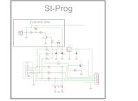
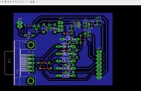
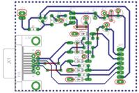
    Si Prog Programmer PCB Design: Eagle Project Review & Feedback for First-Time User Si Prog Programmer PCB Design: Eagle Project Review & Feedback for First-Time User
  • ADVERTISEMENT
  • #2 12399263
    Quarz
    Level 43  
    Hello,
    maciek114411 wrote:
    Hello, I have a request for you to check if I have done everything correctly. This is my first Eagle project so please be understanding.
    It is a Si Prog programmer. I know that the paths would be able to lead better, more minimalist. I will make the plate using the thermal transfer method

    Si Prog Programmer PCB Design: Eagle Project Review & Feedback for First-Time User Si Prog Programmer PCB Design: Eagle Project Review & Feedback for First-Time User
    place here - in a packed form, eg ZIP or RAR, attach the whole project.
    One side of the PCB is not enough to let me check it out.

    greetings
  • #4 12399320
    Quarz
    Level 43  
    maciek114411 wrote:
    Hold on to
    I caught, but you have to wait for the answer, because today is Sunday ...
  • ADVERTISEMENT
  • #5 12399331
    maciek114411
    Level 9  
    Okay, I'm in a hurry :)
  • ADVERTISEMENT
  • #6 12405825
    Quarz
    Level 43  
    Hello,
    maciek114411 wrote:
    I'm in a hurry :)
    it lasted a bit, because I had more urgent matters, and besides, the need was to devote a lot of time to the analysis of this, something here posted.
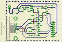
    After removing the black background - tab -> Options / User interface ... / Layout / Backgroud - it looks like this:
    Si Prog Programmer PCB Design: Eagle Project Review & Feedback for First-Time User
    My guess is that the designed PCB is one-sided - I do not see it any other way.
    And then you have unnecessary guides marked as 1 and 2 and a series of pads "hanging in the air" - all this marked in the red rims.

    greetings
  • #7 12406432
    Anonymous
    Anonymous  
  • #8 12406448
    Quarz
    Level 43  
    milosek wrote:
    As for these hanging pads I do not have any objections, because after using the tool Ratsnest the mass field is poured nicely by combining the previously hanging points.
    Only that on - see above - PCB drawing does not show this and no switching on / off layers does not change this.
  • #9 12406571
    Anonymous
    Anonymous  
  • #10 12406598
    Quarz
    Level 43  
    milosek wrote:
    I admit the right but after removing this polygon and applying the above tools all unconnected pads reveal.

    Si Prog Programmer PCB Design: Eagle Project Review & Feedback for First-Time User
    You can not see anything here, that's why I changed the background from black to white - see above - and then you do not see those connections.
    I know it is supposed to be so, but I have to check it and not correct it for the author of the subject, so I proceed formally here and see what I see (or rather do not see).
  • #11 12410217
    maciek114411
    Level 9  
    I do not understand too much what's going on and what to improve. For me, how do I download the file that I previously inserted and I click ratsnest GND is properly spilled and all connections are made. Even the first picture is with properly poured GND. These grommets are not unnecessary, they combine the field of mass. And as for the white background, I changed it and GND is still properly spilled, you had to remove it by mistake. Unfortunately, there is no possibility (or at least I can not) save the file so that after opening the mass field was visible was visible, it is always marked with a broken line and only after clicking ratsnest reveals itself
    I wanted to check the PCB in terms of functioning or how it will build it will work? Does it have any errors?

    Ps. In the picture with the white background that you put in the mass is not visible, therefore it does not prompt you to connect it together but blue dotted lines can be seen, if you click on ratsnest then it would show up.
  • #12 12410231
    Quarz
    Level 43  
    maciek114411 wrote:
    I do not understand too much what's going on and what to improve. For me, how do I download this file that I previously put in and I click ratsnest GND is properly spilled and all connections are made. Even the first picture is with properly poured GND. These grommets are not unnecessary, they combine the field of mass. And as for the white background, I changed it and GND is still properly spilled, you had to remove it by mistake. Unfortunately, there is no possibility (or at least I can not) save the file so that after opening the mass field was visible was visible, it is always marked with an interrupted line and only after clicking ratsnest reveals itself
    I wanted to check the PCB in terms of functioning or how it will build it will work? Does it have any errors?
    Look there: post # 10 , is there something visible there?
    How do I check the correctness of your PCB as I can not see in the connection drawing?
  • #13 12410260
    maciek114411
    Level 9  
    If you want to see all connections, download this PCB file again and after downloading click on ratsnest in eagle
  • #14 12410321
    Quarz
    Level 43  
    maciek114411 wrote:
    If you want to see all connections, download this PCB file again and after downloading click ratsnest in [e] E agl e'u
    Unfortunately, but it does not work for me.
    Show what you see when you change backgrond to Colored , or White - see here my post post # 11 - I can see this invariably like this:
    Si Prog Programmer PCB Design: Eagle Project Review & Feedback for First-Time User
  • #15 12410436
    maciek114411
    Level 9  
    I have marked you with the option you need to click
    Si Prog Programmer PCB Design: Eagle Project Review & Feedback for First-Time User
    And try again, maybe slightly reduce or increase this dotted line and then click on ratsnest. Maybe something got stuck :)
  • ADVERTISEMENT
  • #16 12410455
    Quarz
    Level 43  
    maciek114411 wrote:
    marked you with the option you need to click
    Si Prog Programmer PCB Design: Eagle Project Review & Feedback for First-Time User
    Thank you ... :lol: ... I will check.

    EDIT: It worked, but only when I installed a newer version of Eagle - 6.4.0

    PS See TAM , I've put there the information about a reliable and free tool - Captura 1.0 - for taking screenshots.
  • #17 12410630
    maciek114411
    Level 9  
    So I'm waiting for opinions about PCBs?
    All good?
  • Helpful post
    #18 12410650
    Quarz
    Level 43  
    maciek114411 wrote:
    marked you with the option you need to click
    Si Prog Programmer PCB Design: Eagle Project Review & Feedback for First-Time User
    And try again, maybe slightly reduce or increase this dotted line and then click on ratsnest. Maybe something got stuck :)

    Quarz wrote:
    maciek114411 wrote:
    So I'm waiting for opinions about PCBs?
    All good?
    I will reply at the earliest tomorrow ...
    The PCB design presented above seems to be correct and in accordance with the schematic diagram.
    It would be worth bolding two paths - thinner than the others - from where it is already possible.
  • #19 12415117
    maciek114411
    Level 9  
    I ran the whole path around Jena (I let go under rs232). And in the second I can not do much better with tin than with the pickle.
    Thanks for the help
    And yet someone could write which goldpins is miso sck and reset.
  • Helpful post
    #20 12415176
    Quarz
    Level 43  
    maciek114411 wrote:
    I led one whole path differently (I released it under RS232). And in the second I can not do much better with tin than with the pickle.
    You can do it - put a virtual pad on it and then a thinner path on one side and a thicker one on the other.

    maciek114411 wrote:
    Thanks for your help
    Please ... :lol:

    maciek114411 wrote:
    And yet someone could write which goldpiny is [mosi miso sck and reset] MOSI MISO SCK and RESET .
    View TU - this is the accepted standard - but it does not suit me with the standard adopted there and on the site of the original design SI-Prog is different - see description -> AVR microcontroller adapter
    Consider whether it is worth replacing this single-row connector with a two-row one.
  • #21 12415248
    maciek114411
    Level 9  
    There is a 4 MHz quartz resonator drawn on that diagram, is it superfluous, can not program the microcontroller on the internal oscillator?
  • Helpful post
    #22 12415253
    Quarz
    Level 43  
    maciek114411 wrote:
    There is a 4 MHz quartz resonator drawn on that schematic. Is it superfluous to be able to program the microcontroller on the internal oscillator?
    For this answer question, look in DataSheet for a specific ?CPU.
  • #23 12415263
    maciek114411
    Level 9  
    From what I read, it is not necessary. I will program atmege 8.
    If I had any problems, I will still write.

Topic summary

The discussion revolves around a user's first PCB design project using Eagle software for a Si Prog programmer. The user seeks feedback on their design, particularly regarding the layout and connections. Several participants provide insights, suggesting improvements such as removing unnecessary guides and ensuring proper ground connections. Issues with visibility of connections due to background color settings are addressed, with recommendations to use the Ratsnest tool for revealing connections. The user learns that a 4 MHz quartz resonator may not be necessary for programming the ATmega8 microcontroller, as it can utilize the internal oscillator. Overall, the PCB design is deemed correct, with suggestions for enhancing trace thickness and connector configurations.
Summary generated by the language model.
ADVERTISEMENT