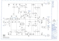
Heath...ok, the quiescent current is set by the circuitry around Q8 which generates a small voltage (about 1.2 volts or so) to bias Q14 and Q15. These transistors DO have those resistors R36 and R37 in their emitter leads so will act as constant current sources, supplying the bases of the 2 or 4 output transistors. When you put 2 output transistors in place of one like this, you don't increase the gain, just the current carrying capability. The currents through the output transistors also flow through R36/R37 but if the voltage across R36/R37 rises, it will tend to cutoff the driver transistors Q 14/15. So it's a self regulating system (pardon the pun Mr Self, I should have said negative feedback

. The bias current for the output transistors will be divided by 2 for 2 transistors, it's a current drive not a voltage drive. it will only be exactly half-half is the output transistors are matched.
If because of using 2 output transistors in each leg you wanted to double the output (current, not voltage) of the amplifier too, you would halve the value of R36/37, for example by putting two 0R1 resistors in parallel. Because they drive the biasing circuitry (and the short circuit protection) you wouldn't have separate resistors for each transistor. But Mr Self is trying to spread the load between the transistors, not increase the output.Low distortion amplifier design is quite an art and Mr Self is very much a master of it.BTW what voltage power rails are used for this amp?
Thanks // David


