logo elektroda
logo elektroda
X
logo elektroda

What Are the Missing Components Near JL1 and PD101 on This PCB? (Photos Included)

lakiernik175 345 3
ADVERTISEMENT
Treść została przetłumaczona polish » english Zobacz oryginalną wersję tematu
  • #1 21346780
    lakiernik175
    Level 11  
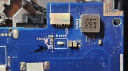
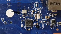
    Hi. This thread is old but I will try to join here with a request. I have a board that works something but not quite. After visually inspecting it I discovered missing components in two places on the board from the top. Bottom left corner next to the USB ports a row of components next to JL1 and bottom right corner opposite, one component next to PD101. Perhaps someone would be so kind as to advise what I should solder in. Thank you in advance for your kindness Close-up of a circuit board with missing components near markings JL1 and PD101. Fragment of a blue printed circuit board with missing components near the PD101 and PJ602 labels. .
  • ADVERTISEMENT
  • #2 21346819
    Stani12
    Level 28  
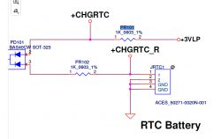
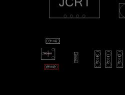
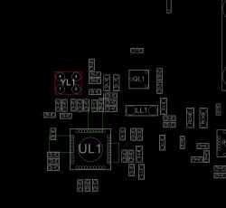
    Here you have everything.
    There are no components next to YL1.
    Electrical circuit diagram for an RTC battery. PCB diagram with designated component spots and labels, no elements next to YL1. Schematic of an electronic circuit with component labels, YL1 is empty. .
  • ADVERTISEMENT
  • #3 21346849
    lakiernik175
    Level 11  
    Thank you. Now I know what is missing. Now just the values.
    PR101 1K resistor
    Still need:
    CL29
    CL21
    CL20
    Below two places RL11 and RL4 but I think they were empty?
  • Helpful post
    #4 21346942
    dt1
    Admin of Computers group
    CL20 = 1uF 6.3V 0402
    CL21 = 0.1uF 16V 0402
    CL29 = 15pF 50V 0402

    RL11 and RL4 and RL9 empty by default, this is space for optional 4.7k 5% resistors 0402.
ADVERTISEMENT