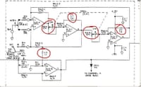
Ok.
I have checked out the circuit, admittedly for just a minute... I will continue
First observations:
_____________________________________________________________________________________________________________
Cd and Ce are simple bypass capacitors, the purpose of these capacitors is to shunt noise on the power supply
line to ground and to allow the opamp to source current instantaneously. I would advise every stage be populated
with the 0.1uF capacitors specified while keeping the voltage rating at a minimum of 25V and the package as
small as possible. There is no go reason for the "NOT USED" except for cost cutting. Every stage needs these
capacitors... furthermore, if you use single opamp packages (as I often would recommend in these types of
circuits) I would use the same bypass technique on each package. I would strongly advise using tantalum or
ceramic capacitors in these positions.
Section Cd , Ce
1 0.1uF (minimum Voltage rating of 25V and smallest package possible)
2 ""
3 ""
4 ""
_____________________________________________________________________________________________________________
Cf is simply a coupling capacitor. For the low frequencies you need higher capacitance to allow the signal to be
properly coupled, it seems to me that all capacitors in the Cf range are seriously small for that application.
Provided you are going to use decent opamps, I would use a minimum of a 10uF cap for Cf and I would be tempted
to make it much higher than that... possibly by using two or more 10uF in parallel, I could see myself using 4
of these caps in parallel for proper coupling. (Realize that even with an infinite valued capacitor in this
position, the opamp will still see a 100k load). I would strongly advise using tantalum or ceramic capacitors in
these positions with a minimum working voltage of 36V and the smallest package possible... it might be more cost
effective to use smaller caps and put a bunch of them in parallel.
Section Cf
1 10uF (possibly up to 40uF would be good, minimum Voltage rating of 36V and smallest package
possible)
2 ""
3 ""
4 ""
_____________________________________________________________________________________________________________
At this point, we only have one variable: the value of Ca and Cb for each stage... it turns out that these are
always the same for each stage.
So... In the end, I am short of time these days so I simulated the circuit.
I made sure the Q controls functioned properly before narrowing the bandwidth as much as possible, I did this to more accurately find the center frequency.
Once I narrowed the bandwidth, I then tuned the circuit to the lowest center frequency available and the highest center frequency available and recorded them in the following table:
C = capacitance in Farads
Fl = lowest center frequency tuning
Fh = highest center frequency tuning
C Fl Fh
-----------------------------------------
100.0E-9 26.0E+0 340.0E+0
27.5E-9 97.0E+0 1.2E+3
8.0E-9 333.0E+0 4.3E+3
2.2E-9 1.2E+3 15.4E+3
I also plotted this data in a log-log plot and it looks to be very reasonable and no suprises turned up...
I have attached the log-log plot in case you wish to extrapolate values from it.
The bottom axis represents capacitance in Farads, the vertical axis represents the center frequency... the two lines correspond to the maximum center frequency (Fh) and minimum center frequency (Fl) available with respect to the selected capacitance value for this circuit.
I simulated all 4 capacitance values listed... and they are logarithmically equidistant, and the bandwidth remains logarithmically equidistant.... (logarithmically equidistant means they are visually equally spaced on a logarithmic plot)
Remember, this graph is in log-log format and you might want to learn how to read one very well before you attempt to understand it.


