Power Supply Design Notes: Your First Boost Converter
Boost converters are useful devices for designers because they solve a number of power problems at low, medium and high voltages. If it is necessary to reach a certain voltage, which might be higher then the one available, a voltage step-up converter will solve the issues. A boost converter, or step-up converter, is nothing more than a direct current (DC) to direct current (DC) converter, which increases the input voltage to obtain a higher voltage on the output load. Obviously the price to pay is a decrease in the available current, since the power P = V * I cannot change.
How a boost converter works
Boost converters are a class of switching power supplies that contain two active semiconductor components (a diode and a transistor or MOSFET) and some energy storage elements such as the capacitor and inductor (see the principle diagram in
Figure 1). To reduce the voltage ripple, filters consisting of capacitors can be added to the output of the converter. The voltage gain depends on the duty cycle, the value of the inductor, the input voltage, the switching period and the output current. In the system there are two distinct logic states of the switching element:
• in ON state, the MOSFET is closed and the current on the inductor increases;
• in OFF state, the MOSFET is open and the inductor current flows through the diode, the capacitor and the load.
If the switching element works very quickly, the inductor does not completely discharge and there will always be a voltage that is higher than that of the input even when the MOSFET is open. During the OFF time, the blocking diode prevents the capacitor from discharging through the MOSFET. This whole process has to happen very quickly.
 Figure 1: The basic diagram of a boost converter
 Our DC / DC voltage booster must have the following electrical characteristics:
• input voltage: 12 VDC;
• output voltage: 24 VDC;
• power: 150 W;
• switching frequency: 30 kHz.
In theory, two 12 VDC batteries connected in series could be used, but the size, weight and cost of the system would increase dramatically. The switching frequency exceeds the human hearing threshold and avoids the production of any
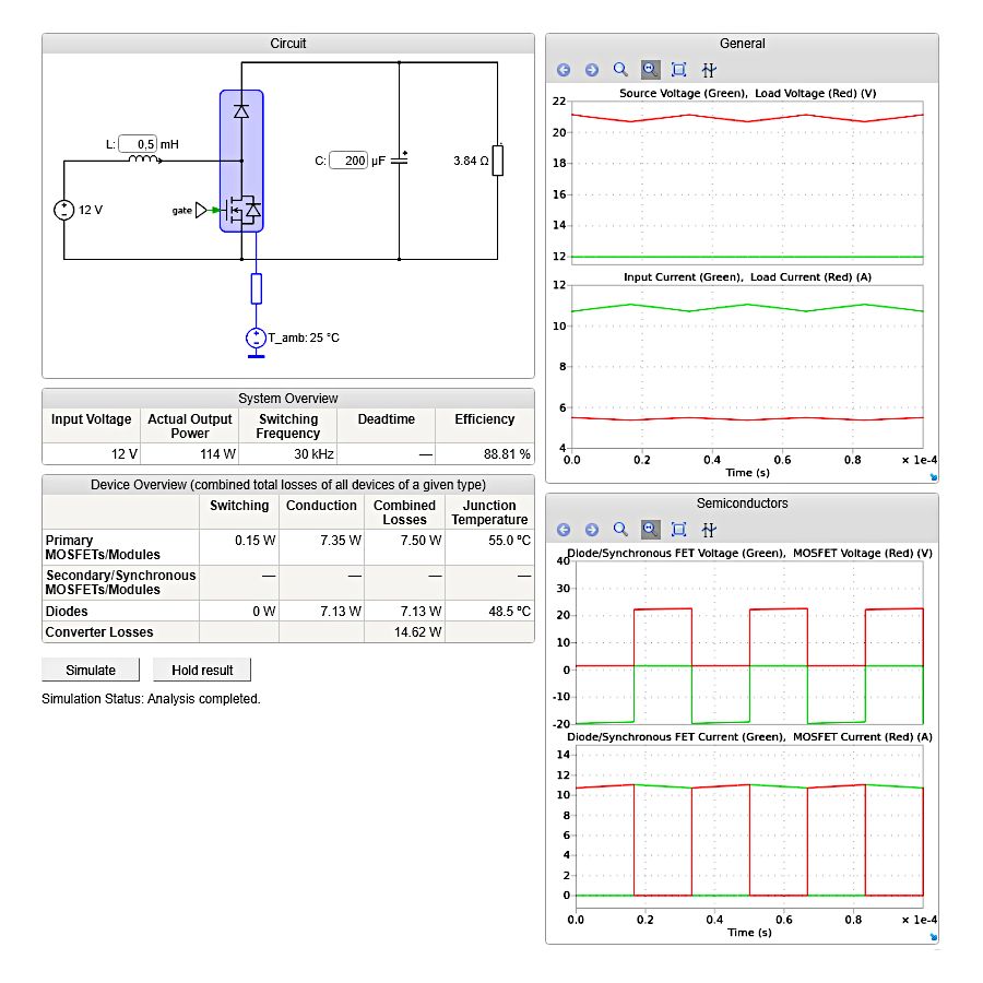
whistles. The online calculator used is able to generate a complete summary (
see figure 2) which shows all the main characteristics of the circuit.
Figure 2: The useful summary page generated by the online calculator
Online calculators
The quality of a boost circuit depends on many factors, first of all the type of SiC MOSFET and SiC Schottky diode used. The sizing of the components is quite complex and must include many behaviors, both static and dynamic. To facilitate the work of designers, there are many online tools and calculators that help in calculating the elements to be used in the wiring diagram. One of these is the powerful “SpeedFit 2.0 Design Simulator” made available by Wolfspeed, a subsidiary of Cree. The calculator can be used free of charge and is available at
www.wolfspeed.com/speedfit. It divides the design of the power supply into several steps:
• choice of the type of converter (DC / DC, AC / DC, DC / AC);
• input of the data (voltages, power and switching frequency) and choice of the sub-category (this choice also shows the principle diagram);
• choice of SiC devices (MOSFETs, diodes and any modules);
• choice of system thermal parameters (information on the heatsink such as insulation, temperature, thermal resistance, time constant, ambient temperature and any additional heat sources);
• execution of the simulation, in which the values of the components used and the graphs of the voltages and currents are shown, as shown in figure 3;
• production of the final summary, in which all the details of the circuit are highlighted, including voltage, power and current data, the semiconductor devices used, operating losses and some thermal data.
The calculator also includes a guide that describes in detail all the operations to follow.
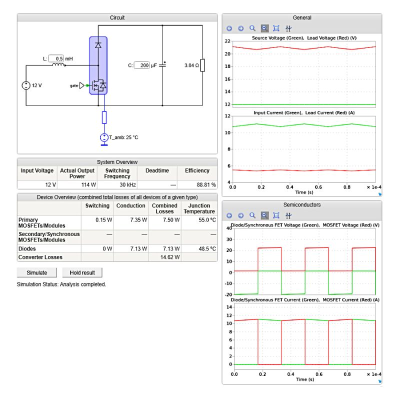 Figure 3: The online calculator allows a very simple and fast configuration of the converter
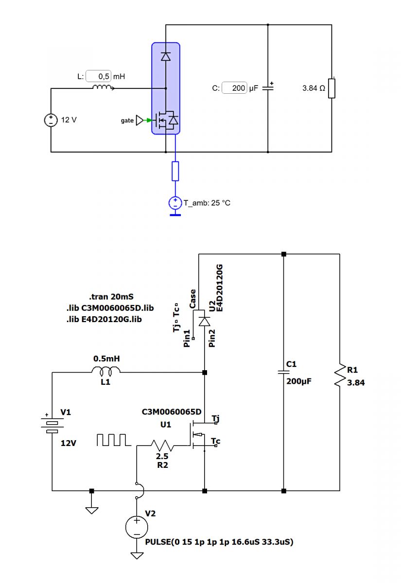
The scheme of the project
After having entered all the information in the Web calculator, the system immediately provides the results and the values of the components to be used, as shown in
figure 4. The same wiring diagram has also been reproduced on the LTspice simulation software, for the execution of different static and dynamic simulations. Remember that a complex simulation with LTspice (or other simulators) with the presence of inductors and external components is extremely slow and could take a few hours to obtain the final results. The electrical components used are the following:
• V1: 12 V battery;
• V2: 0-15V (zero-peak) square wave generator with a frequency of 30 kHz and a duty cycle of 50%. The voltage of 15 V is dictated by the MOSFET datasheet as the recommended gate voltage;
• R1: load;
• R2: resistance of 2.5 Ohm;
• L1: inductor of 0.5 mH;
• C1: 200 uF electrolytic capacitor;
• U1: C3M0060065D SiC Mosfet;
• U2: Schottky diode C3D16060D (another more performing model, the E4D20120G, was used in the diagram).
The site provides users with SPICE models of MOSFETs and Schottky diodes, ready to be incorporated and used with their favorite electronic simulation program. The pins “Tc” and “Tj” are reserved, respectively, to set the component container temperature and the junction temperature. This will be covered in an upcoming tutorial.
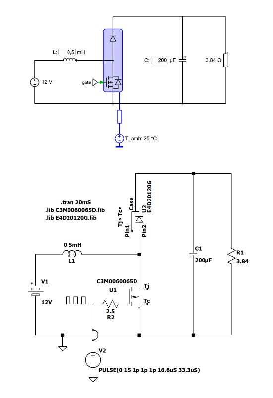 Figure 4: Wiring diagram of the Boost converter, proposed by the Speedfit calculator and drawn with LTspice
Simulation of the output voltage
The first interesting simulation involves verifying the output voltage of 24 V, a voltage which is nominal since it will actually be slightly lower. The simulation, carried out at the ends of the load R1 and of the electrolytic capacitor C1, took about four minutes (the SPICE models are quite complex). The relative voltage transient graph appears in its entirety in
figure 5. The real transient ends in about 7 ms. After that, the power supply is fully operational and works regularly. As you can see, the graph also shows the response curves of the online simulator, which correspond perfectly to the results of LTspice.
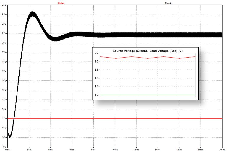 Figure 5: Output voltage of the Boost converter is almost double compared to the input
One of the disadvantages of switching power supplies is that they generate noise and interference due to the fast switching signal that occurs inside the electronic components. Appropriate filters added to the output eliminate or mitigate this issue. As can be seen from the spectrogram in
figure 6, on the output signal shows the following harmonics which are, however, tolerable by most of the loads:
• 30 kHz (-20 dB);
• 90 kHz (-37 dB);
• 150 kHz (-45 dB);
• 210 kHz (-51 dB);
• 270 kHz (-55 dB);
• 330 kHz (-61 dB);
• 390 kHz (-64 dB);
• etc.
These are harmonics with very low entities, which in a linear scale would not be at all perceptible. You would just see the harmonic of 30 kHz (94 mVRMS), of 90 kHz (12 mVRMS) and of 150 kHz (5 mVRMS).
 Figure 6: Harmonics on the output signal due to the switching of the active elements
One of the most important data of a switching converter circuit is undoubtedly efficiency. Greater efficiency means greater use of available energy and less losses, resulting in cut on costs and cleanliness of the environment. The equation for calculating the efficiency of an electrical circuit is very simple:
and in particular, with regard to our electrical circuit:
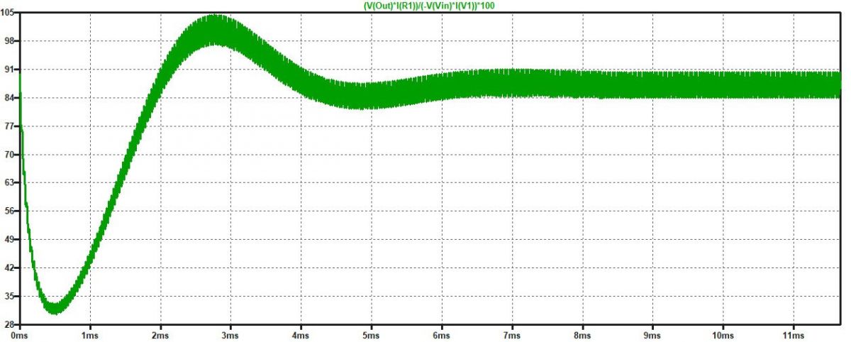
The simulation returns an efficiency value of 87.05%, not much different from the 88.81% expected and shown on the online calculator. The efficiency graph in a transient of 12 ms is shown in
figure 7.
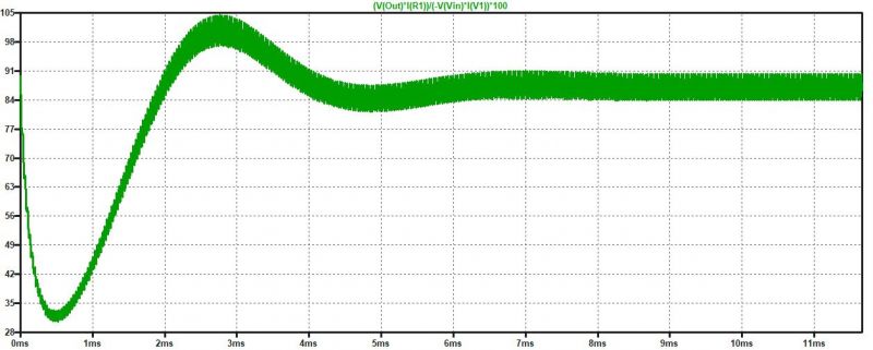 Figure 7: Transient graph of the circuit efficiency
Conclusions
The boost conversion circuit is very simple in its basic version, and can also be performed with discrete components of any type. To improve its performance, it is always important to choose high-quality components, characterized by a high-switching speed of the logic states, a high ability to manage high currents and a low Rds (on) to minimize power and heat dissipation. The circuit is represented in its minimal and generic version. It can be modified according to your needs.


Comments