Ever wondered what sits in the Flash memory from a modern TV? I invite you to a short presentation of the inside of the Samsung UE55MU6452U 55" 4K UHD Smart TV combined with reverse engineering and emulation of the T-Con controller firmware. Here I will show how such a TV is built, how its backlighting is realised and what components can be recovered from inside. Finally, I will also try to rip the contents of the Flash memory from inside, decode it properly, determine its architecture, UART addresses and fire it up in a simple emulator.
Disassembly and backlighting
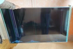
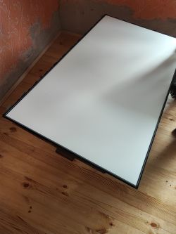
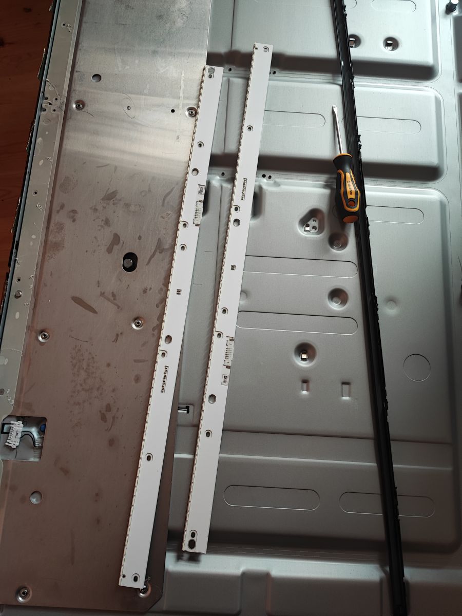
I started the disassembly with the screen itself. In LCD TVs, the image is generated by the liquid crystal matrix, while the backlighting is a separate module behind it. This used to be implemented using CCFL fluorescent tubes, but now we have LED TVs. The LED strip is only on the bottom edge of this unit, but their light passes through several layers of diffusers and diffuser films that evenly illuminate the entire panel surface.
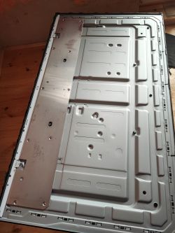

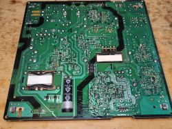
With the back cover removed, you can see the two main modules of the TV - the power supply and the motherboard. There are also, of course, the speakers.
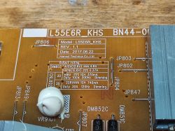
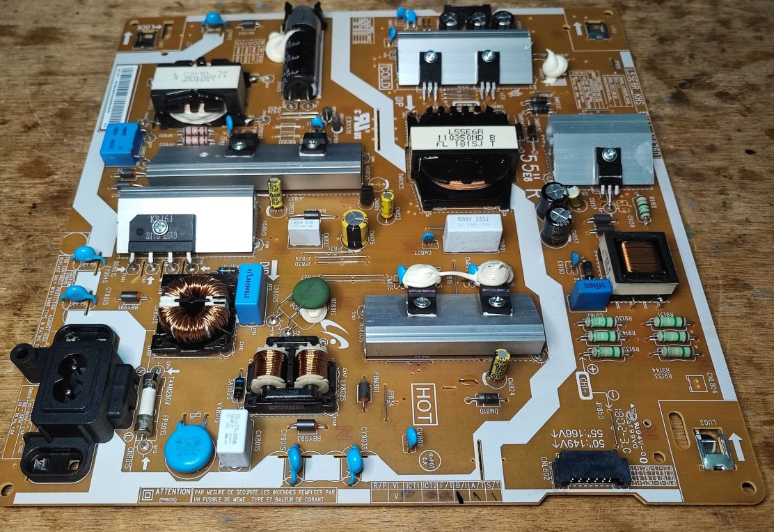
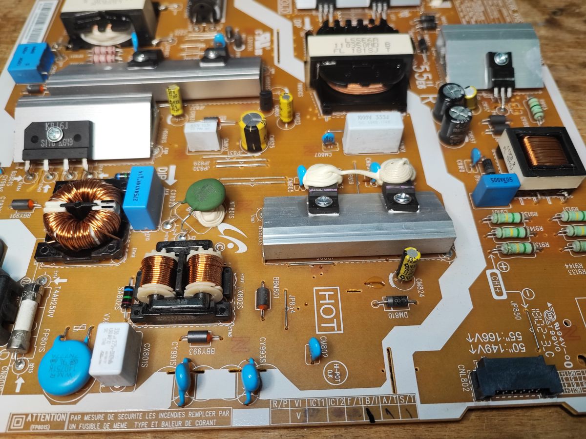
Power supply L55E6R_KHS
The power supply is essentially built from two modules. Here we have a separate power supply for the motherboard, in this case 12.8 V at just over 5 A, and separately we have a constant-current power supply for the LED backlight, depending on the version this can be 198 V 370 mA at 300 Hz.
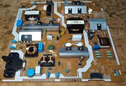
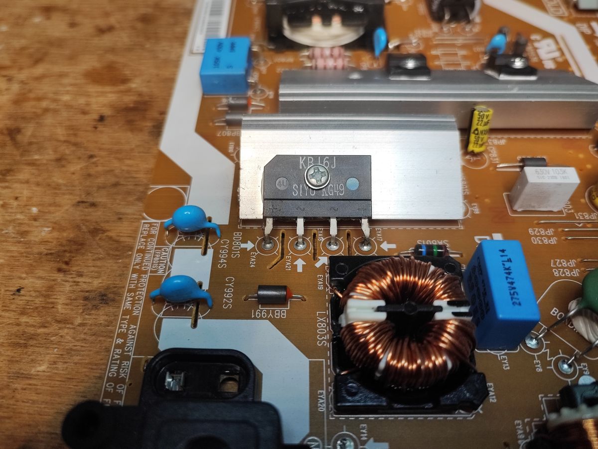
These types of power supplies are usually single-sided boards. Some of the components, especially the larger ones, are threaded and some, including the ICs, are SMT. Interestingly, the pulse transformers and the 400 V capacitor have been specially mounted in the PCB cutouts to reduce the height of the PCB.
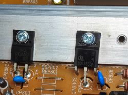


Of the components here, we have 10N60M2 MOSFETs, 60S380CE transistors and U10A6C1 ultrafast diodes.
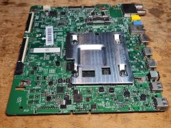
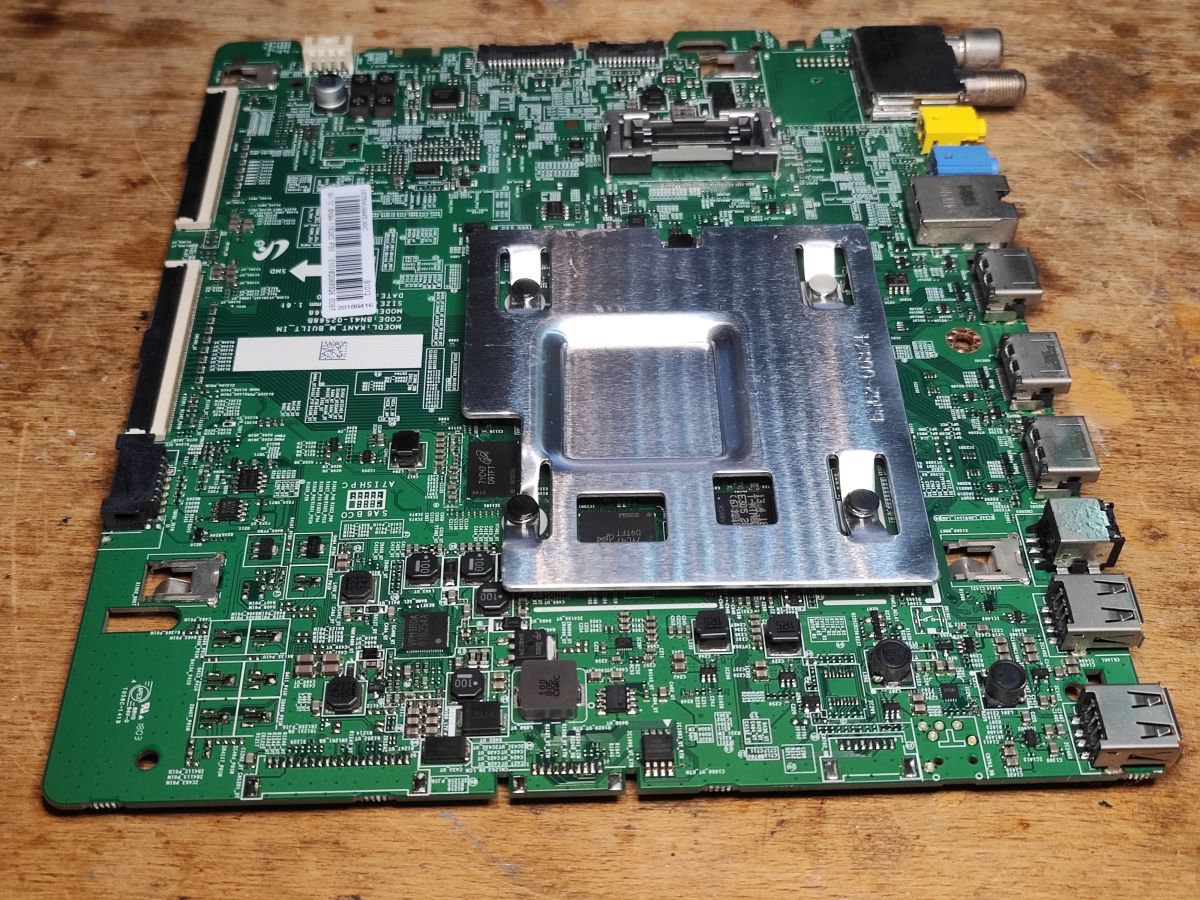
Mainboard
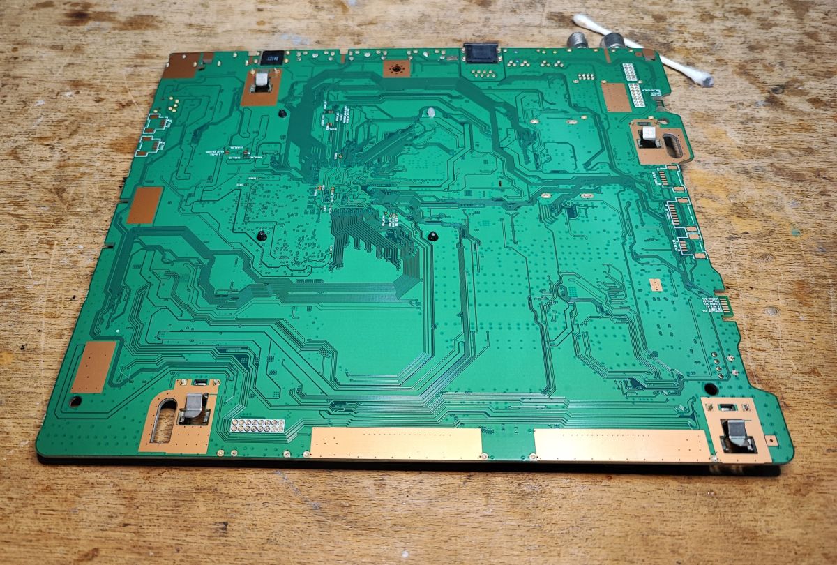
The motherboard is realised using surface mount. The PCB is double-sided, but the components are only on the top. What we have here is essentially a small computer, complete with processor, memories, inverter and I/O section.

The loudspeakers are driven by a TAS5749M class-D audio amplifier:

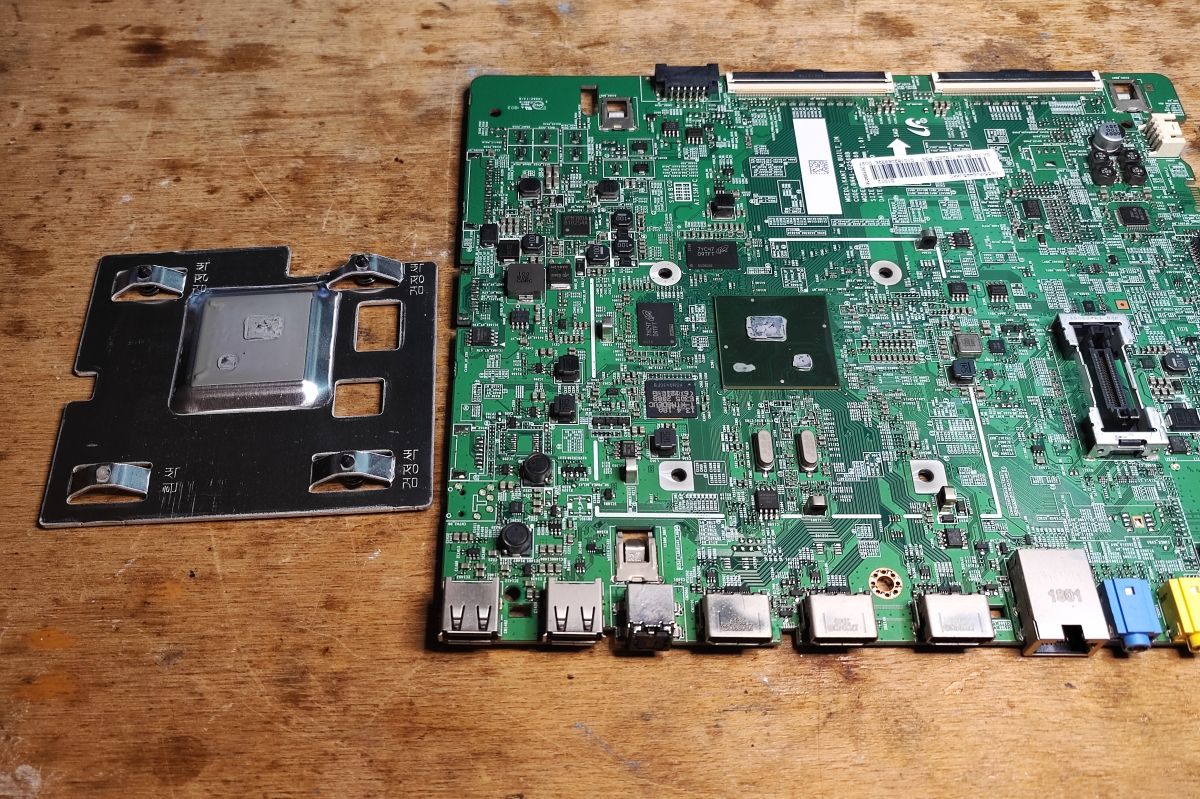
With the heatsink removed:

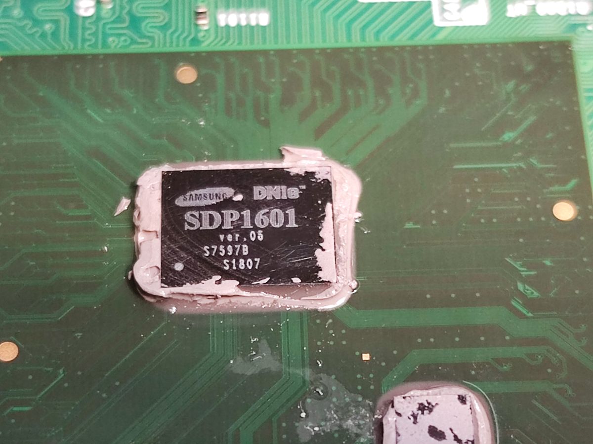
Components such as the CPU, RAM and Flash are already assembled using BGA (Ball Grid Array) technology. This provides higher interconnect packing density, better electrical properties and a more compact chip design, while unfortunately making manual repair and soldering of these components more difficult.

After cleaning the paste, the CPU can be identified - SDP1601 ver. 05:

I couldn't find any information about it on the web, except for a wikimedia page with a gallery from a rather similar TV:
https://commons.wikimedia.org/wiki/File:Samsu...E40MU6409U_-_board_-_Samsung_SDP1601-5286.jpg
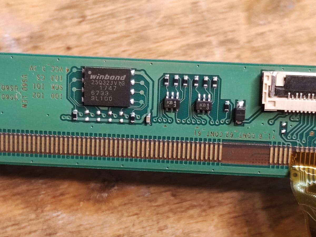
Flash memory from T-Con?
The T-Con (Timing Controller) is the controller that controls the LCD matrix and is responsible, among other things, for generating control signals for the pixels. The first bone of the 25Q80DVSIG is located at the edge of the PCB. Its SPI line leads to the pads from the missing connector.

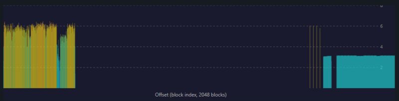
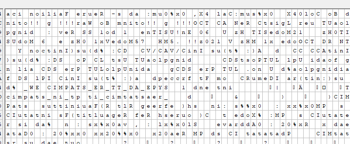
The data entropy is quite high, but only up to offset 0x19000. Beyond that, the memory is empty.
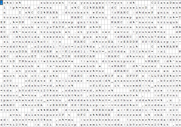
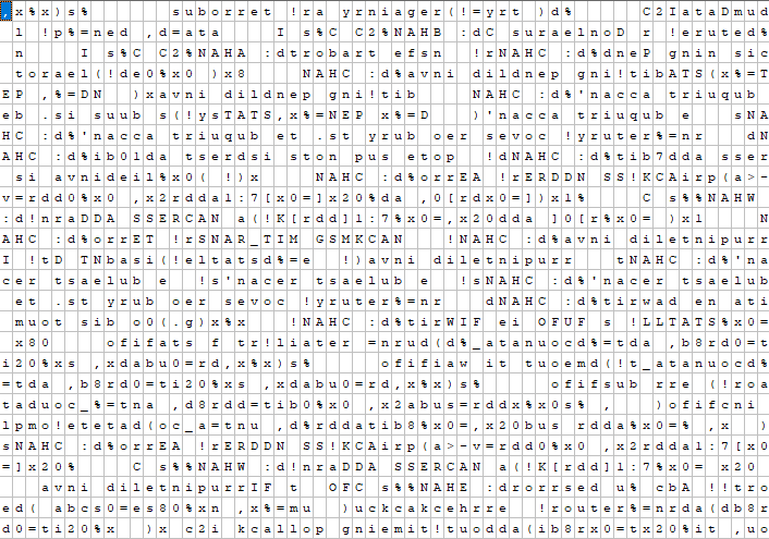
Here I've already found some interesting sections that look like subtitles, but in some strange language. Or maybe something is messed up?

A quick analysis of the letters shows that we have the byte order changed. I have given examples to confirm my idea in the table:
| Rough (as in file) | | Decoded (32-bit byte-swap) |
| | locnIcerrhc tskce | Incorrect checksum |
| oB dnito!! g | Booting!!! |
| | CIMPATS_ER_TT_DA_EPYS | SYS_TYPE_AD_TT_RE_STAM PIC |
| NOCTamI I eg ofns% | TCON Image Info sd% |
I made a program to flip all the bytes:
In the subtitles I found information about the processor - aeabi Cortex-M0. In addition, there are a lot of error messages, about Flash memory and about T-Con:
0x00884F:  Current Task ID : %d, BaseSP:0x%08x, SP:0x%08x, Name:%s
0x008889: [Task %02d] BaseSP:0x%08x, SP:0x%08x,StkSize:Assert Remain:[%06d][%06d], ID:%02d, Name:%s
0x0088E4: -----------------------------------------------------------
0x008921: Oops!!! HardFault_Handler
0x00893C: TIME : Preempt : %d us, OneCmd Op :%d us
0x00899A: OutPut Hz :
0x0089A7: 60 Hz
0x0089AF: 120 Hz
0x0089B8: idle
0x0089BD: user_debug
0x0089C8: usr_boot_main
0x0089D6: Enter Multi Tasking
0x0089EB: UART RDY
0x0089F5: TIMESTAMP : %s
0x008A05: 20170825_0922
0x008A13: I2C M Init
0x008A1F: sf_wp_check
0x008A2C: MEMIF_CMD_SRAM_REFLASH
0x008A44: Current Version : 0x%02X
0x008A5E: Release Date : 0x%06X
0x00AFDC: ----------FGT Status Information---------
0x00B007: init_skip : 0x%04x
0x00B01B: fw_model : 0x%04x
0x00B02E: test_mode : 0x%04x
0x00B042: chip_ids : 0x%04x
0x00B055: chip_corner : 0x%04x
0x00B06B: chip_revision : 0x%04x
0x00B083: booting_done : 0x%04x
0x00B19C: Source Address : 0x%08x
0x00B1B5: Err Size:0x%x
0x00B1C4: Header CRC : 0x%x, Result CRC Val:0x%x
It also looks like there is a command line:
0x00B40D:  Input 1. Register, 2. Print list, 3. Select Remove Register, 4. All Remove Register, 5. Trace Start, 99.Exit :
0x00B47E: Full!!!
0x00B487: Register Address[%d] :
0x00B49F: [%02d] Addr:0x%08x, Val:0x%08x
0x00B4BF: Remove Line :
0x00B4CE: Select [ 1.Debug Buffer Mode] or[ 2. Print Mode] ??? :
0x00B506: Stop!!!
0x00B50F: [%08d]Temperature : %d'C
0x00B529: [Test] 1: Trace OneCommand Toggle
0x00B54C: [Test] 2: UART ReInit
0x00B563: [Test] 3: Access Address
0x00B57D: [Test] 4: Trace Address
0x00B596: [Test] 5: manual onecmd
0x00B5AF: [Test] 6: DBG Buffer Mode
0x00B5CA: [Test] 7: Force Booting Done
0x00B5E8: [Test] 8: OSD Image
0x00B5FD: [Test] 9: DDR RW Limit Check
0x00B61B: [Test] 10: IDLE Task Monitoring On/Off
0x00B643: [Test] 11: SPI Flash RW Limit Check
0x00B668: [Test] 15: 3DC 60
0x00B67B: [Test] 17: TCON CRC
0x00B691: [Test] 18: EW DDR Test
0x00B6AA: [Test] 19: Temperature Test
0x00B6C8: [Test] 98 : FT Status Info
0x00B6E4: [Test] 99 : Exit
0x00B6F6: [Test] Input :
Various types of Flash are supported:
0x00B730: w25x10
0x00B768: w25x20
0x00B7A0: w25x40
0x00B7D8: w25x80
0x00B810: w25q80
0x00B848: w25x16
0x00B880: w25q16
0x00B8B8: w25x32
0x00B8F0: w25q32
0x00B928: w25x64
0x00B960: w25q64
0x00B998: w25q32
0x00B9D0: w25q64
0x00BA08: gd25q32c
0x00BA40: gd25q32c
0x00BB94: SF[%d]:%s, JEDEC ID : 0x%x,
0x00BBB1: Quad Mode
0x00BBBC: Single Mode
0x00BBC9: SF[%d]: No Exist : 0x%08x
What is Demura? Demura is an LCD matrix calibration technique that compensates for brightness and colour imbalances between individual pixels. The correction data is usually stored as LUT arrays.
0x014DF6: Fail / Retry
0x014E04: TCON Demura Register Data Uploading
0x014E29: fail - Incorrect checksum / Read : 0x%X / Calc : 0x%X
0x014E60: TCON Demura LUT Data Uploading
0x014E80: fail - Incorrect checksum / Read : 0x%x / Calc : 0x%x
0x014EB7: ACC FCnt Init
0x014EC6: Demura bypass
0x014ED5: No Demura Image
0x014EE7: Write Fcnt ISR Routine
0x014EFF: M49B6U0Fxx
LUT? Lookup table? But what is an SDC? Is it about colour mapping?
0x015201: 120Hz Vx1 Mode
0x015211: TCON RDY
0x01521B: Tcon Init(us): %d
0x01522E: DCC/VCC/VA Init(us): %d
0x015247: ACC
0x01524C: ACC Init(us): %d
0x01525E: SDC Post LUT Uploading
0x015278: SDC Post LUT Uploading fail
0x015294: SDC Pre LUT Uploading
0x0152AD: SDC Pre LUT no.%d Uploading fail
0x0152CE: SDC IP Init(us): %d
0x0152E3: accept from FRC
0x0152F4: Demura Init(us): %d
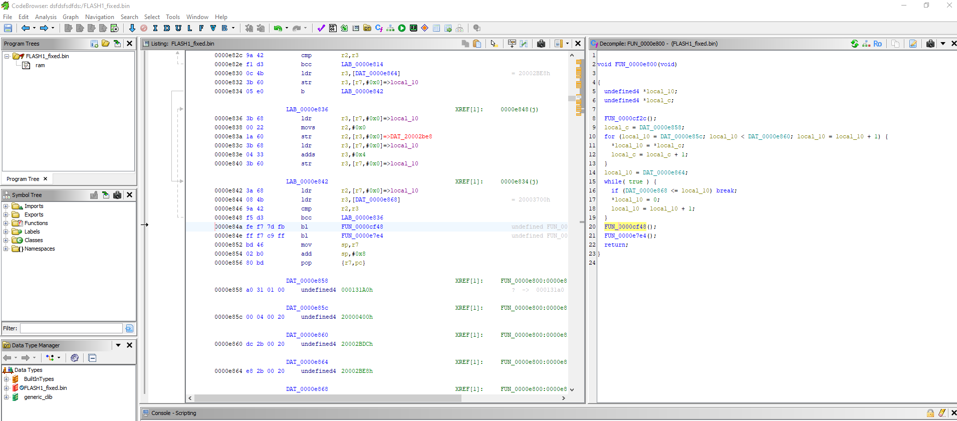
I loaded the Flash into Ghidr, used the ARM:LE:32:Cortex settings. The instructions and functions are decoded correctly.
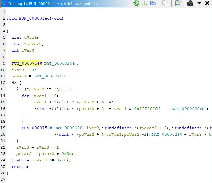
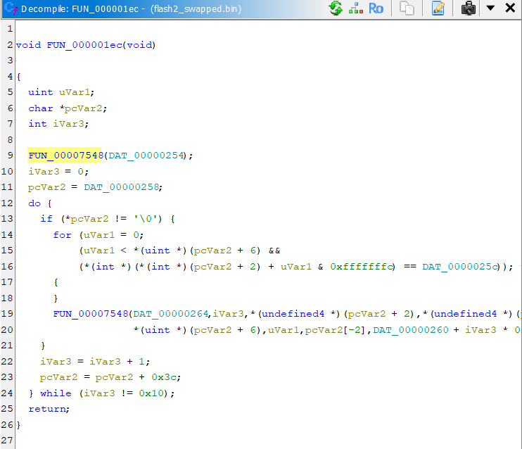
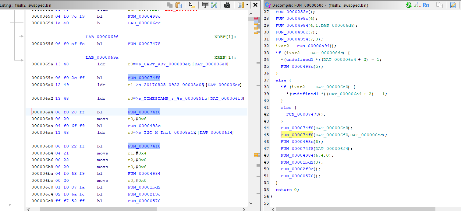
You can quickly find there references to subtitles, for example to UART_RDY, in the screenshot below we have the ldr instruction which loads a pointer to this subtitle, just after that the 74f8 function is called. I wonder what it can do with this write....

A first glance doesn't explain it yet, but let's not give up:

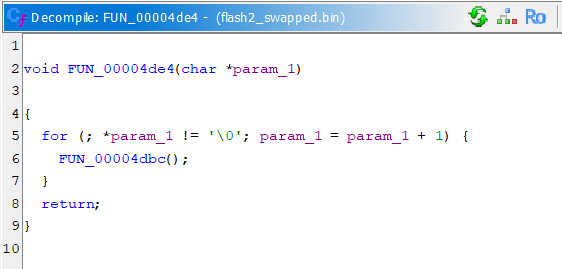
One of the subfunctions looks like an iteration of a null-terminated byte:

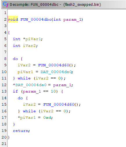
Each character is processed by another routine, which first seems to wait in a loop until the UART is free, and then sends one byte:

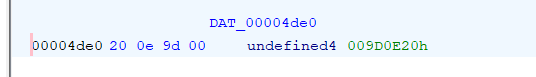
FUN_00004d60 just examines lighting the third bit on the value with address DAT_00004d6c. Ready flag? Whereas something writes to the value with DAT_00004de0.... but DAT_00004de0 is a pointer, what is there in memory?

There is the address of the UART_TX_DATA register there, that is 0x009D0E20! It is this register that continues to send characters. Similarly, the other registers can be specified:
- 0x009D0E00 = UART_CTRL (on/off, value 0x3)
- 0x009D0E04 = UART_BAUD (baud, value 0x3085)
- 0x009D0E10 = UART_STATUS (bit 2 = TX ready)
- 0x009D0E20 = UART_TX_DATA (byte to be sent)
- 0x009D0E28 = UART_FIFO_CFG (FIFO depth 0x50?)
The correctness of this can only be verified.
Flash memory from T-Con - part 3 - emulation
Finally, I prepared a simple
emulator PoC (Proof of concept) in Capstone deassembler and Unicorn emulator in Python. In addition, the whole thing emulates basic peripherals and has patches for some instructions. I captured operations on the extracted UART registers. The result is the following boot log:
  Captured output (237 bytes):
  ────────────────────────────────────────────────────────────
UART RDY
TIMESTAMP : 20170825_0922
#I2C M Init
.SF[0]: No Exist : 0x00000000
KTCON Image Info : M55A6U1F20
hTCON Register LUT uploading done
Warm Booting !!!!!
USIT En!
60Hz USIT Mode
USIT Phy 0 Init done
USIT Phy 1 Init done
PMIC Write
  ────────────────────────────────────────────────────────────
This confirms the identification of the registers and gives hope that, after compiling the firmware ourselves, we would also be able to display text.
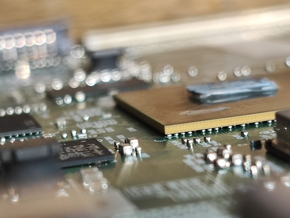
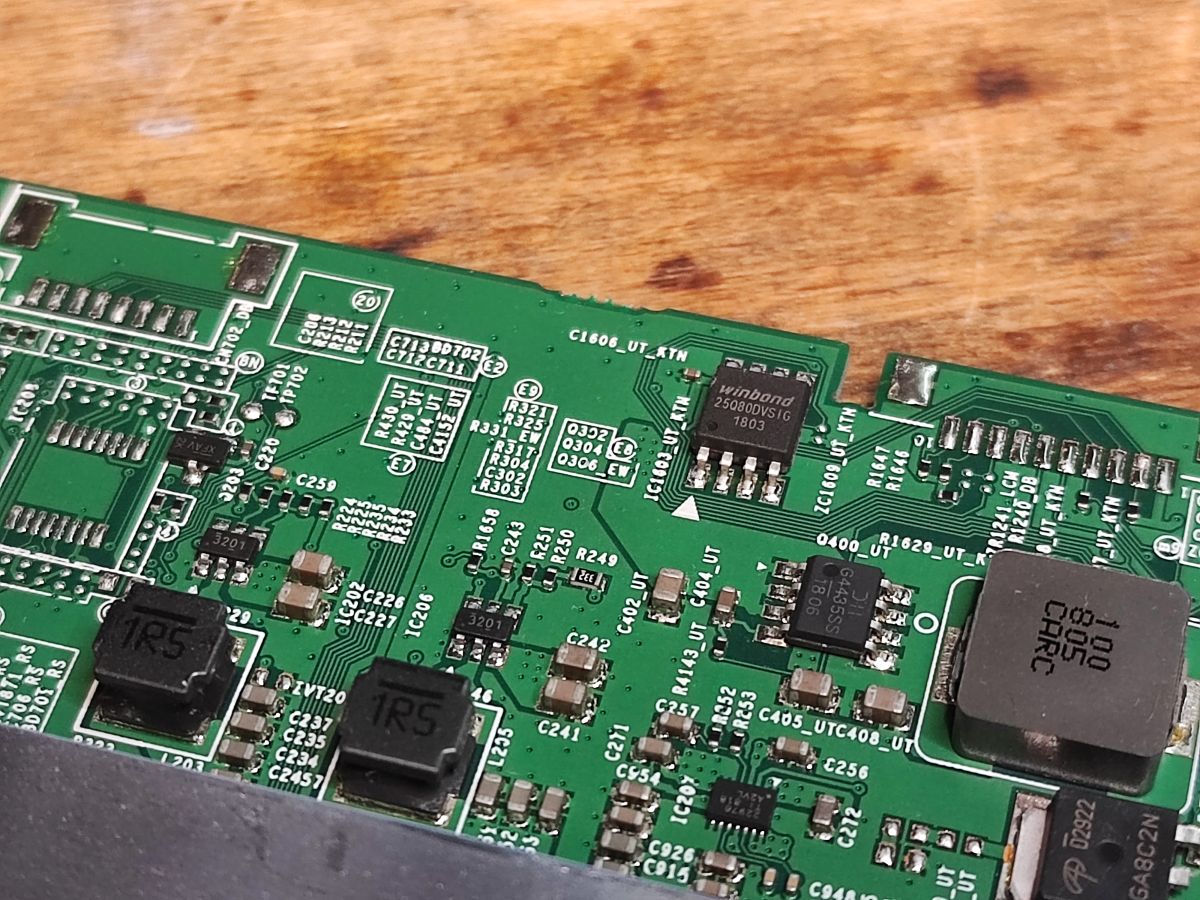
Flash memory at the CPU
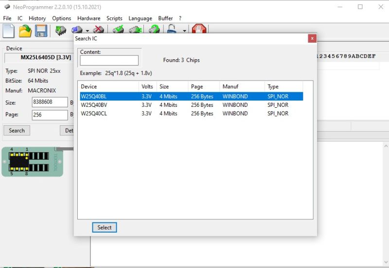
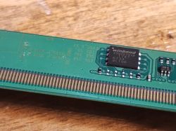
The second Flash memory found is located right next to the CPU. Its designation is 25Q40CLSIP, from which its size can be deduced: 512 KB. I was betting that here, as on the PC, sits some BIOS.
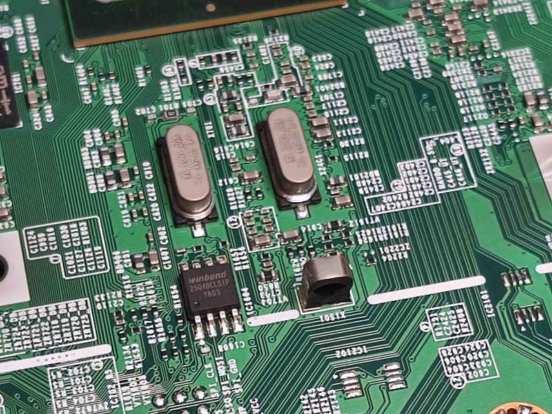
I desoldered and ripped it down using CH341:
I started with an entropy analysis. Entropy is a measure of the disorderliness of data - the higher it is, the more random the bits in memory are. In the context of flash memory, it allows you to quickly assess which bits are ordered and which bits contain random or compressed data.
Here, too, the subtitles are rearranged:
You can quickly find interesting identifiers. Compilation date:
Image Info: Ver: %04 Build Date:  %s[%s] - e
Date: Sep 25, 2017  Time: 6:07:12
I2C bus:
I2C CHAN%d: FIFO CTR=0x%08x, DBG=0x%08x, DATA=0x%08x, STA=0x%08x
I2C CHAN%d: CORE CON=0x%03x, STAT=0x%02x, ADDR=0x%02x, DS=0x%02x, CONE=0x%02x
I2C CHAN%d: INTR PEND=0x%02x, MAS ENK(=0x%02x)
I2C CHAN%d: P%d.SCL(%d) direction=%s, len=, level=
I2C CHAN%d: P%d.SDA(%d) direction=%s, len=, level=
HDMI (Consumer Electronics Control) CEC controller:
RX_ERROR Pend 0! a:
RX_ERROR FIFO Flush O Fl timeout!
RX_NACK Pend 0! a:
RX_NACK FIFO Flush O Fl timeout!
CEC CHANGE: %dLine%d(P)%d.direction=%level, s
ADC messages:
ASR: ADC%d not EOC pending%d
A!: ADC%d not interrupt pending! 0x%x%s
[%ums]: ADC%ld %ums Timeout! EOC(0x%08x, INT 0x%08x) %s
AD: value C0 0x%
ADC value 1 0x%0
ADC2 value 0 0x%08xS: %s
MiCom - communication with the microcontroller?
MiCom ON Assign not ready already own . 0x
ResetMasterWait: %s timeout! wait count %unt %is
od: as already assigned not AON Mic . om 0x%x%s
ow: gen timeout %l(t)suu 0x!
Here too everything loads nicely into Ghidr when ARM Cortex mode is selected, Little Endian byte order. I also reverse the words beforehand so that the subtitles look correct:

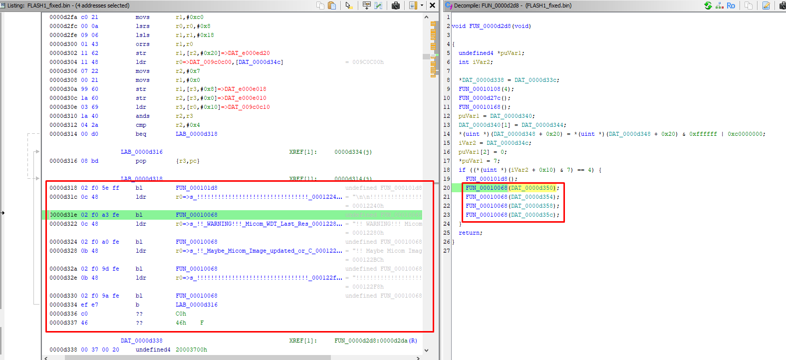
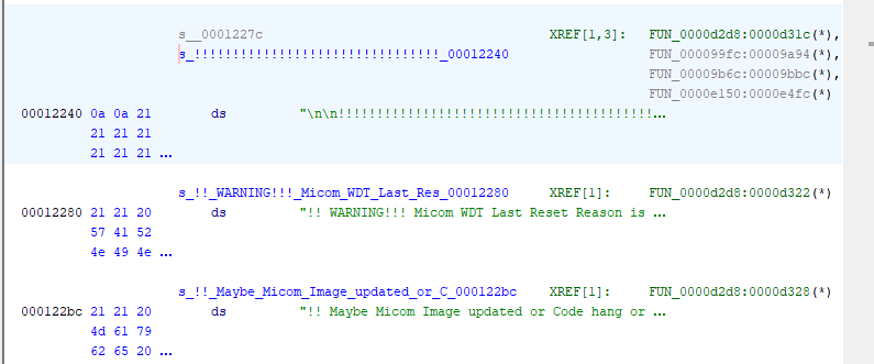
The more important functions are even more eye-catching. Let's take a look at this random code snippet for example - what is FUN_00010068?
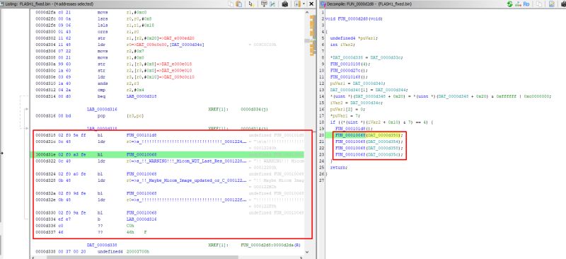
It's probably displaying error messages, the argument is a Flash write:
 Third Flash memory
Finally, a little curiosity - there was also a memory bone on the matrix itself, but I did not keep it after disassembly and did not examine its contents. I need to do this on my next TV:
 Summary
What a surprise, this was supposed to be a presentation of the inside of a TV, and along the way it turned into attempts to reverse-engineer flash memory from TCON. In a similar way, it also managed to slightly decode the other memory, the one around the CPU. Both were characterised by byte reversals in the words, as could be seen from the various messages left behind. After performing a simple 32-bit byte-swap, the words in the memory began to arrange themselves into intelligible texts, which made firmware analysis much easier. This made it possible to establish that the T-Con controller uses an ARM Cortex-M0 processor and to identify parts of the multitasking system and UART support. The code analysis also identified the addresses of the UART registers, making it possible to create a simple Proof-of-Concept emulator that can capture the firmware boot log. The second Flash memory, the one next to the CPU, I spent slightly less time on, but it looks like a small initialisation firmware. In its contents you can find support for various peripherals such as I2C, HDMI-CEC or ADC, as well as communication with an additional microcontroller. It is not, however, a BIOS.
Ultimately, it turns out that even individual TV modules have their own microcontrollers and firmware, which can be analysed just like other embedded systems. Even a simple analysis of the binaries can reveal quite a lot of information about the operation of the entire device.
The results are quite encouraging and give hope, in a way, for compiling and running one's own programme on this type of chip. Even a simple LED flashing classic would be enough to start with, although analysis of the UART also gives hope of displaying custom messages. Perhaps I will also attempt such a thing, although I admit that I must first find a board where the clip from CH341 works, or find a way to program without dumping the memory, because, however, repeatedly re-soldering circuits somewhat increases the time-consumption of such a game.
I don't know how much I'll divide myself yet in the context of this particular board, but I already have a few others in stock, complete and working, from smash-and-grab TVs, and there I've determined that there is room for experimentation.
Will it be possible to turn a TV into an Arduino? We will find out soon enough!


Comments
On what circuit is the head i.e. the RF module? Can you see it in one of the photos? [Read more]
Are you thinking of any RF project? https://obrazki.elektroda.pl/1386192500_1777988167_thumb.jpg https://obrazki.elektroda.pl/3785397700_1777988167_thumb.jpg I also have more interesting... [Read more]
Unfortunately, I have not been able to find even the slightest mention of these circuits. It's a pity, because there are even connectors - probably for testing through which it would probably be possible... [Read more]
I'm most limited for now by this flashing slow, in the sense, in the circuit to me CH341 doesn't want to catch in most cases. I don't know if I won't think about some combination like a custom board with... [Read more]
The Si2110-FM gives MPEG-TS as its output. There is even a whole datasheet. In theory, you could cut it off from the CPU and hook it up to a Rapsberry PI to program it via I2C and decode MPEG-TS. In this... [Read more]
And roughly what kind of layouts are you looking for? Going back a bit more to the topic from the first post, I've been investigating another TV board, this time from Manta - the LED4004, and there... [Read more]
It could be something that has a "normal" p.h. output like the R820T, or the MxL5007 (a very good chip) or a "zero IF", or IQ like the AV2012. The circuits can be with DVB-T/C and DVB-S. There is a... [Read more]
These bytes inverted in a 32-bit word are the so-called Endiannes (byte order), this has a historical significance and in principle 2 encodings Little-Endian and Big-endian are used in different processors. ARM... [Read more]
Apparently I've known about Endiannes for a long time, on various systems even when serialising files I've had to invert bytes of integer/float types, just as in Ghidra I set this when decoding instructions,... [Read more]
This was actually invisible to the programmers or operators of the computer in question. The problem arose from the technical way in which memory was attached to the processor, if the processor operated... [Read more]
@pkaczmarek2 On the board you still have the eMMC memory where the whole OS sits. I've seen 4Gb and 8Gb sizes of these memories on Samsungs. If you are stubborn you can read them in the SD card reader... [Read more]
Has a colleague tested this method or just watched others succeed? Fortunately, china already offers very cheap modules dedicated under eMMC literally in the price of an SD reader and you do not need to... [Read more]
Yes, I confirm it works, but.... not with all readers. Of the four I had at the time, only one worked, it was probably a GL838 ripped out of some printer. [Read more]
Very interesting post. Thanks for such analysis and reverse engineering, description of methods. It is helpful. Great job and a piece of work you've done, it's clear t.v. like t.v., but exploring the topic... [Read more]
I look forward to a more in-depth analysis of the firmware. I know manual analysis is tedious work, but have you tried to identify features with known signatures? Or even better - use the GhidrAssist plugin... [Read more]
What program would a colleague recommend for reading/writing eMMC and verifying compatibility? [Read more]
I won't recommend any. I did it once just for fun, to see if it would work. The chip, was an eMMC+RAM combo from some old Samsung on android. When plugged into the reader, it reported in windows as unformatted... [Read more]
I also usually use a USB-eMMC adapter for this, although this way you only access the USER partition of the memory. I used an XGecu type programmer to read the BOOT and RPMB. [Read more]