

logo elektroda
logo elektroda
X
logo elektroda

Simple clock on PIC12F683 - three pins, two I2C buses - DS1307 + FD650

p.kaczmarek2 1233 1

TL;DR

  • A tiny clock uses a PIC12F683, a recycled FD650 four-digit 7-segment module, and a DS1307 RTC.
  • Because the FD650 ignores normal I2C addressing, the design splits the bus into two SDA lines with a shared SCL and separate bit-banged I2C functions.
  • The PIC12F683 has only 128 bytes of RAM, and the FD650 display traffic includes 0x11 at address 0x48 plus digit writes at 0x68, 0x6A, 0x6C, 0x6E.
  • The clock works, time is counted down and displayed, and logic-analyzer captures confirm clean DS1307 reads and display transactions.
  • Memory pressure forced the code to be rewritten with functions moved into the main loop and variables reduced, showing how tight the PIC12F683 budget is.
Generated by the language model.
ADVERTISEMENT
This content has been translated flag-pl » flag-en View the original version here
📢 Listen (AI):
  • Simple clock on PIC12F683 - three pins, two I2C buses - DS1307 + FD650
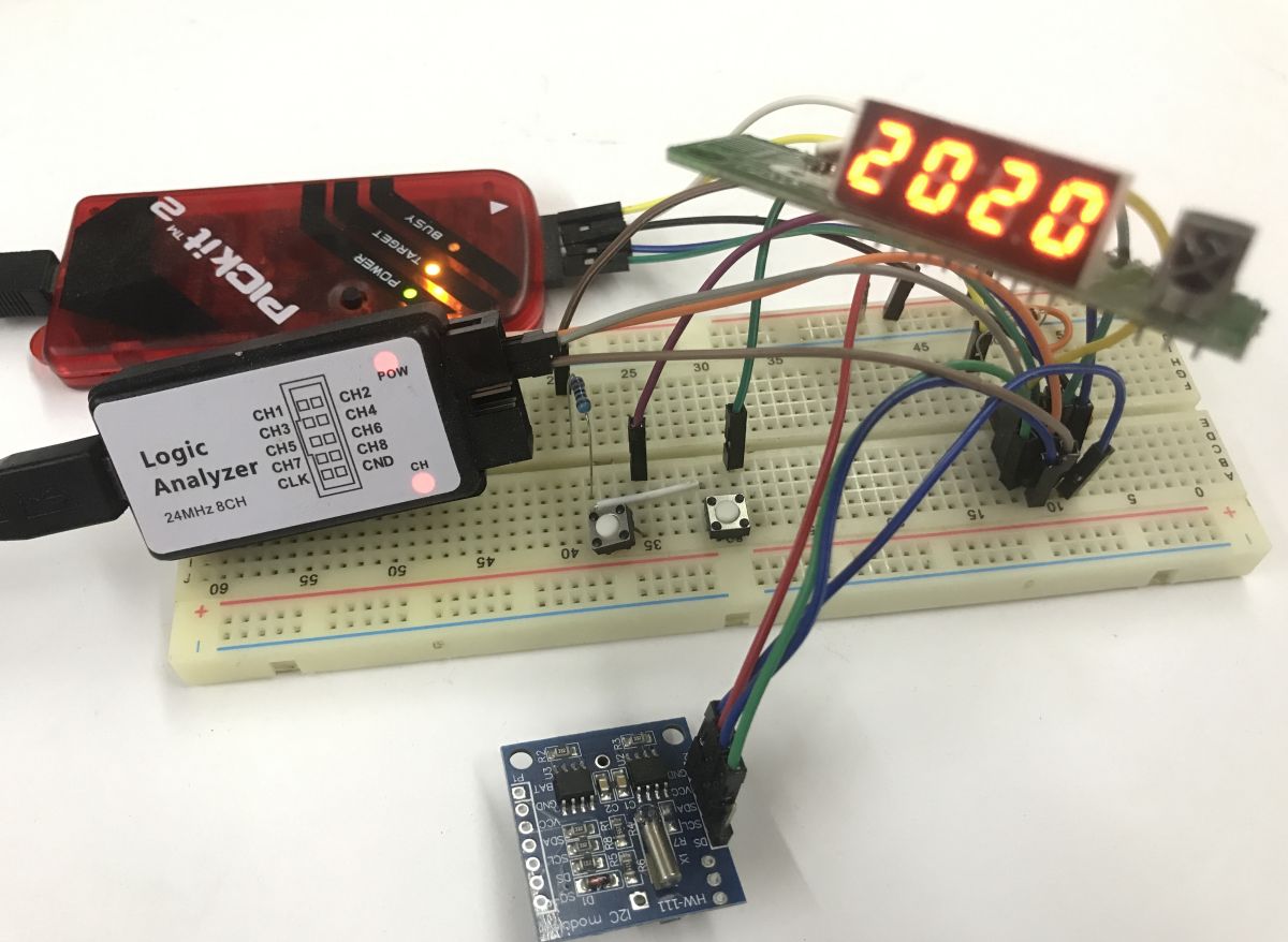
    Today we are building a tiny clock with time keeping, we will realise it based on an 8-bit PIC12F683 microcontroller with only 128 bytes of RAM, a 7-segment display module with FD650 controller recovered from electro-junk and a DS1307 RTC clock. I will also show full waveforms from I2C communication captured with a logic analyser in the theme.

    Why not one I2C bus?
    Let's start with the most important design problem and the obvious question that probably occurs to everyone after reading the introduction to this topic - why two I2C buses at all? Is it not possible to use addresses?
    Unfortunately, it so happens that a large number of popular Chinese chips do not fully adhere to the I2C standard and do not support addressing - there, the first byte sent is not the address of the individual chip, but e.g. a command or immediately the address of the register on which we operate.
    There is a similar problem with the FD650, on which I based this design. The FD650 is a clone of the TM1650, it also appears under the name HD2015. I have already described it extensively in a topic:
    Running the HD2015 display/button controller after reverse engineering, comparison with TM1637
    The FD650 has the very affliction that it will interfere with our other addresses on the bus.
    The other element used in the project, the DS1307, is fully I2C-compatible and doesn't do the problem, but so what?
    The bus needs to be split - I decided to have two SDA data lines and a common clock SCL .

    Organisation of work
    The project is quite complex, so for simplicity I did the first stages on an Arduino. This was primarily dictated by the desire to check that my module from the FD650 survived the operation. Only after making sure that everything is ok with it will I transfer the code to the PIC.

    Module from FD650
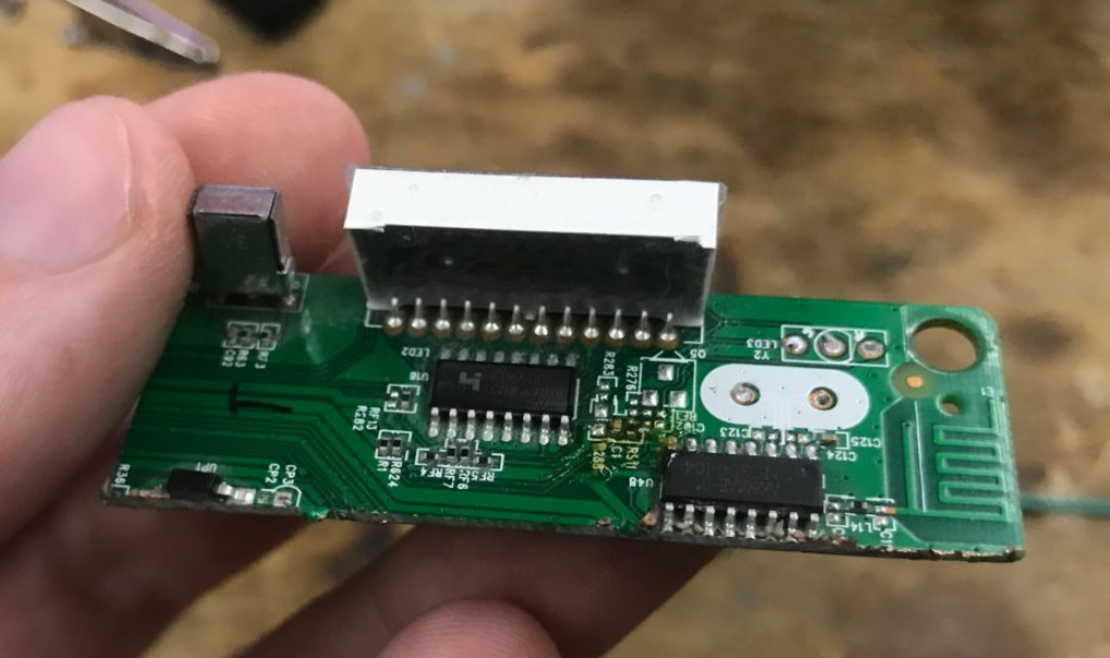
    I recovered the module from an old terrestrial TV receiver. The equipment had no remote control and no longer supported the newer standards with DVB-T2. I've been receiving this type of equipment quite often for a while now, so I've been recovering parts from them in bulk. I didn't have room for another board, so I took the liberty of cutting out only what I could use:
    Simple clock on PIC12F683 - three pins, two I2C buses - DS1307 + FD650
    In addition to the four-digit 7-segment display, there is also its controller, FD650, and some circuitry from RF (unnecessary here - to be removed).
    Simple clock on PIC12F683 - three pins, two I2C buses - DS1307 + FD650
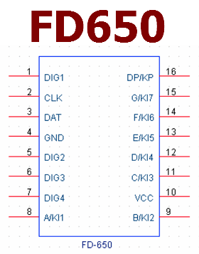
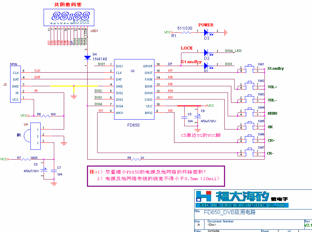
    The circuit on the board may seem incomplete, but nothing could be further from the truth. The FD650 really needs very few components to operate. Below is a sample application of it, which is pretty much in line with what I have on the board. I have only removed the buttons.
    Simple clock on PIC12F683 - three pins, two I2C buses - DS1307 + FD650
    As you can see, you don't even need many resistors - just the 2 kΩ one from the buttons. The LED display doesn't need extra resistors at all.


    I2C scan from FD650
    You don't have to take my word for it though. A simple I2C scan is easy to run, just poll consecutive addresses and check the ACK signal. I implemented this on an Arduino for convenience. I didn't even need to give an external pull up resistor (pulling up to the power supply), as the Arduino allows you to configure the pin in this mode. The polling is done in a loop and the active ones are written out to the UART:
    Code: C / C++
    Log in, to see the code

    There is only FD650 on the bus, but lots of addresses are reported. In line with concerns.
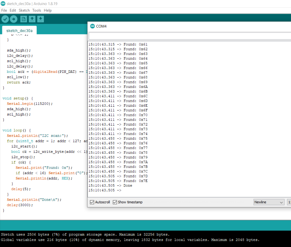
    Simple clock on PIC12F683 - three pins, two I2C buses - DS1307 + FD650
    For verification I disconnected one of the lines - immediately communication is broken:
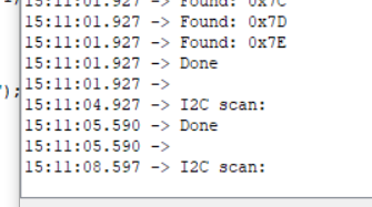
    Simple clock on PIC12F683 - three pins, two I2C buses - DS1307 + FD650

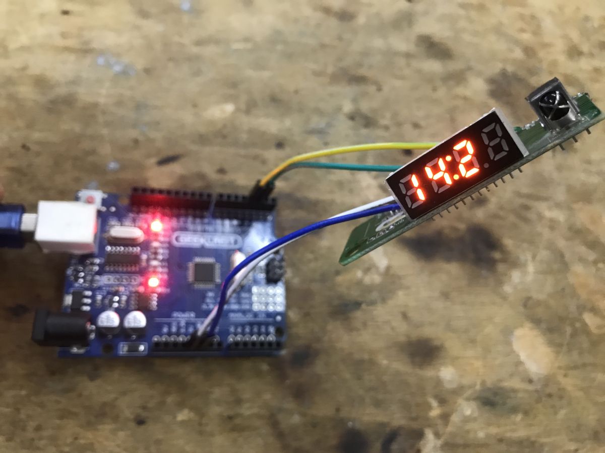
    First segments
    This paragraph will be kept to a minimum as I have essentially repeated this 1:1 work from the previous presentation:
    Running the HD2015 display/button controller after reverse engineering, comparison with TM1637
    Everything went straight away and there was no problem with the segments or font. It looks like the segment-to-pin mapping is standardised here, so that most FD650-based tuners (or devices there?) and clones can share the same operating code.
    Code: C / C++
    Log in, to see the code

    Simple clock on PIC12F683 - three pins, two I2C buses - DS1307 + FD650


    Simple clock
    I then implemented the showTime function, which simply splits the two numeric values into ones and tens, and then sets them to their respective positions and sends them to the display. I don't operate on a string (character string) here, because I would have to manually shift the number and add 0 for the minutes and hours values from 0 to 9.
    Code: C / C++
    Log in, to see the code

    Works:


    Port to PIC12F
    It is time to move the program to the PIC12F. The logic will remain the same, the pin operations will change. On the PIC we directly perform this on the registers. In addition, I set up an internal oscillator for it, such is enough, I have other plans for timing anyway.
    Code: C / C++
    Log in, to see the code

    I don't think these delay_ms are even recalculated to the current oscillator configuration and are skewing, but that's not a problem, there shouldn't be this kind of blocking expectation in the final product anyway. We'll use something better for this.

    Let's focus on the communication itself over I2C for now. It's worth taking a look at what's happening on the bus. I used a logic state analyser for this, I have already presented it in a separate topic:
    Salae 24MHz logic state analyser for £40 - analysis of unknown LED display protocol
    I also added an I2C decoder to the collected data to see the bytes being transferred.
    First, the whole transactions - you can see how the data is sent every (say) 250 ms on the display:
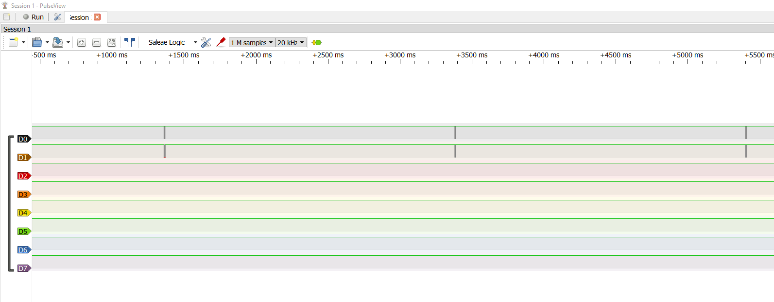
    Simple clock on PIC12F683 - three pins, two I2C buses - DS1307 + FD650
    When zoomed in we see a single operation showTime , this consists of a set of operations to write data to the FD650.
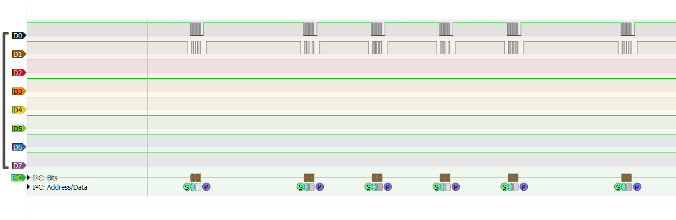
    Simple clock on PIC12F683 - three pins, two I2C buses - DS1307 + FD650
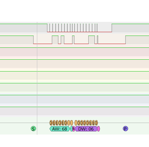
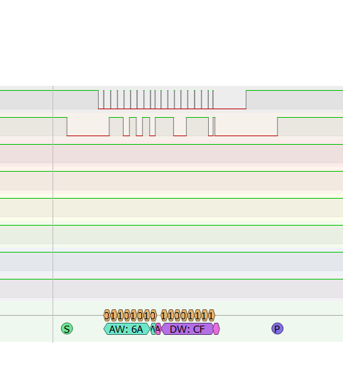
    What we have here is successively running the display (writing 0x11 to address 0x48) and writing four characters (addresses 0x68, 0x6A, 0x6C, 0x6E). The last operation is to re-enable the display - redundant, it was left over from my experiments and I forgot to remove it for the pictures.
    An example close-up of the display enable operation:
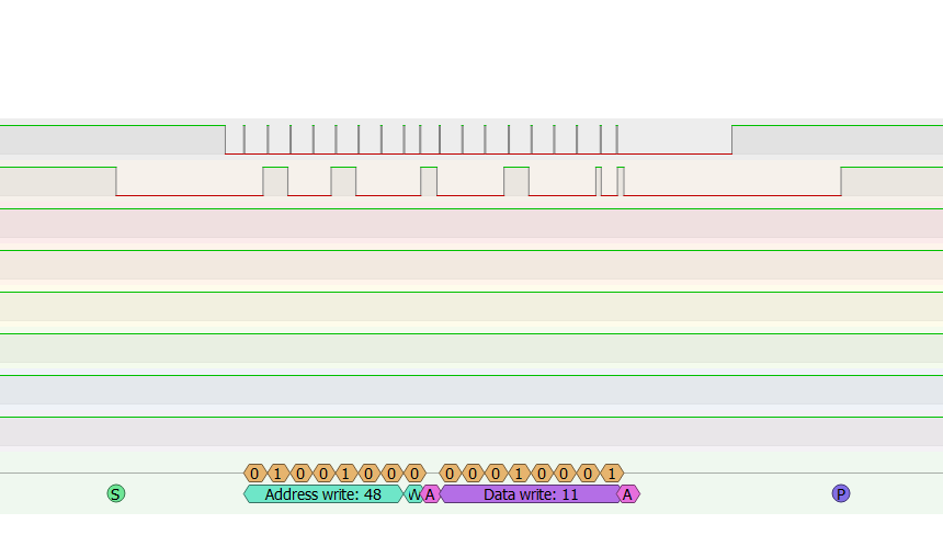
    Simple clock on PIC12F683 - three pins, two I2C buses - DS1307 + FD650
    Similarly, character notation:
    Simple clock on PIC12F683 - three pins, two I2C buses - DS1307 + FD650
    Simple clock on PIC12F683 - three pins, two I2C buses - DS1307 + FD650


    Integrating DS1307
    Now it is time to introduce the DS1307. The DS1307 is a so-called RTC (Real Time Clock), which is a real-time clock chip that is used to keep the current date and time, even when the microcontroller is switched off or reset.
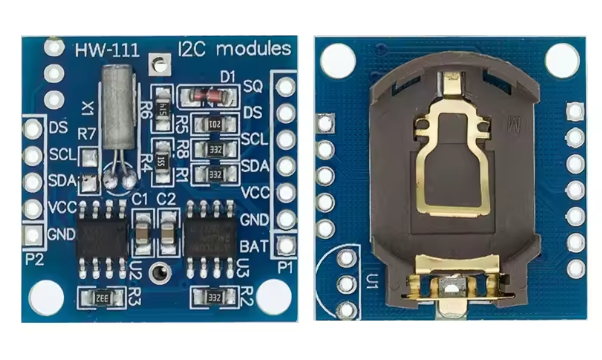
    Simple clock on PIC12F683 - three pins, two I2C buses - DS1307 + FD650
    By using an external backup battery (usually CR2032), the DS1307 can operate independently of the main circuit power supply. Communication with the microcontroller is via I2C.
    My module with the DS1307 still has an EEPROM on board, but I will skip it here for now.
    The whole problem here is that I can't put the DS on the same bus as the FD650, because the FD650 doesn't support addressing in principle and takes up all addresses - I showed this in the paragraph "I2C scan with FD650".
    For this reason I have introduced dividing the bus , as announced.
    Now:
    - SDA of the display is pin 0
    - sCL common is pin 2
    - SDA of the clock is pin 1
    To save memory, I broke the DRY (Don't Repeat Yourself) rule and prepared two sets of I2C functions - one for pin 0, the other for pin 1.
    Code: C / C++
    Log in, to see the code

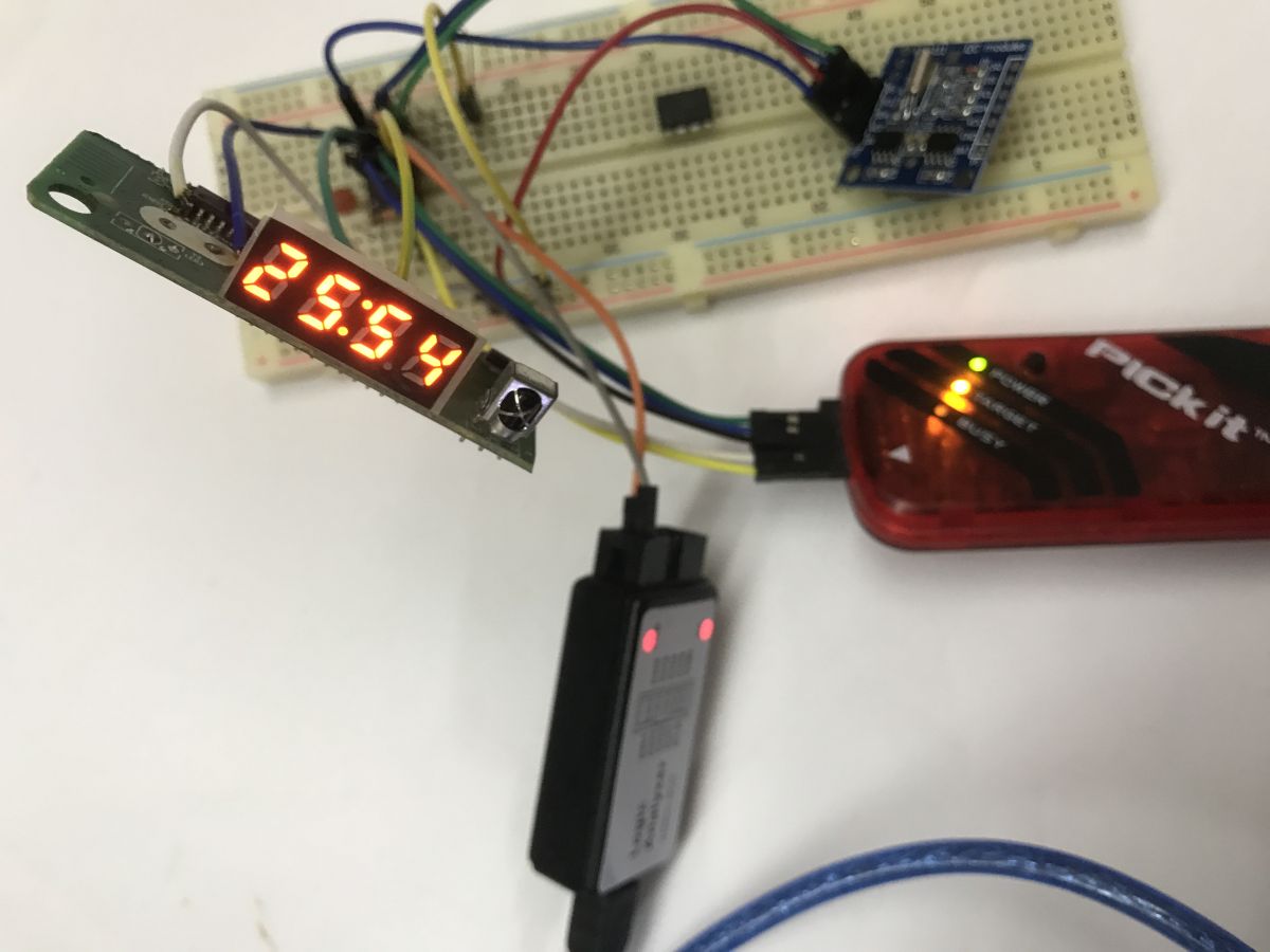
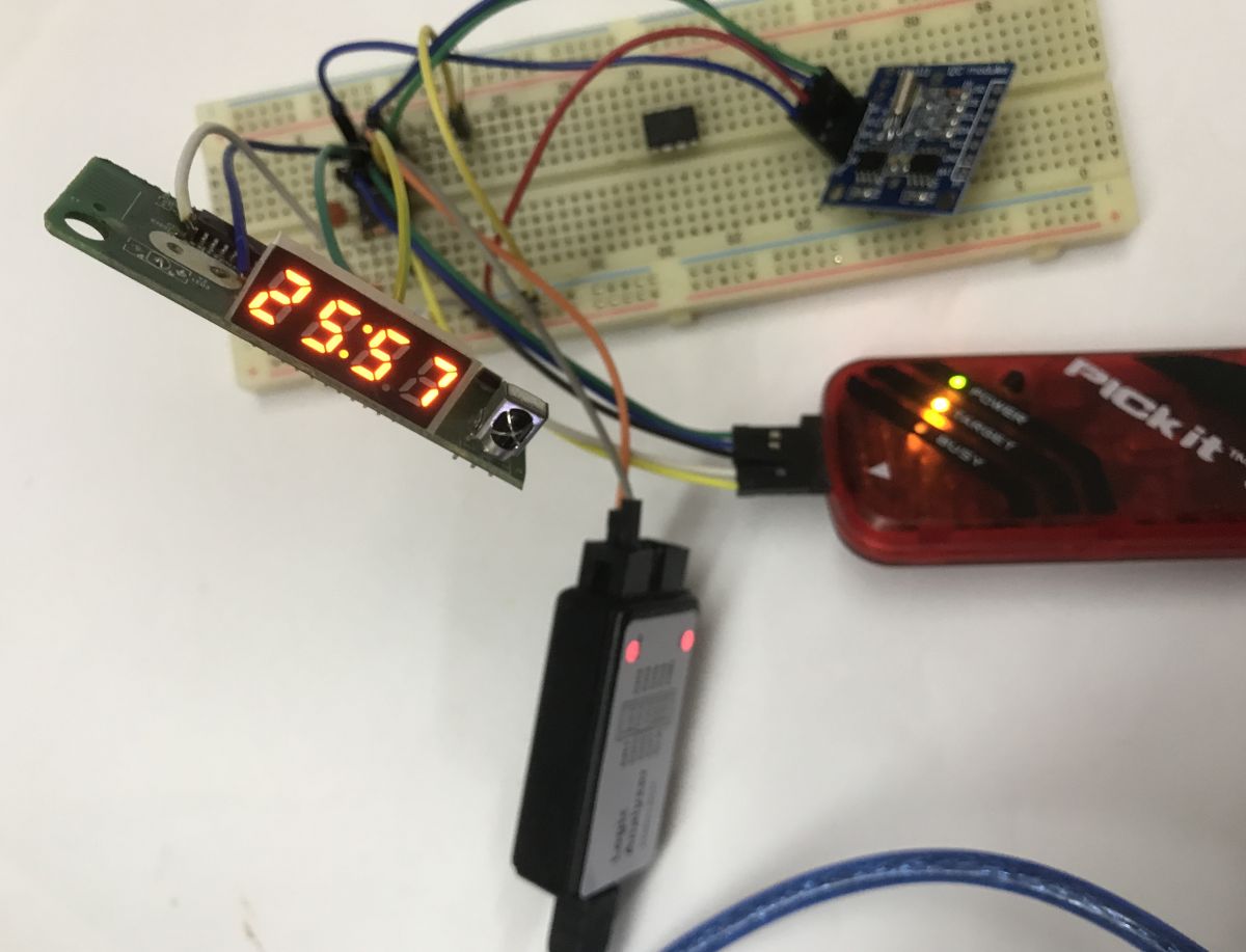
    The pull up resistors turned out to be unnecessary again - the ones from the PIC are sufficient. The code shown works - the time is counted down and displayed. Previously the RTC had to be programmed once, but for now let's assume we did it manually, separately....
    The pictures show the time in mm:ss format, so it may seem odd, but it's more convenient to test this way.
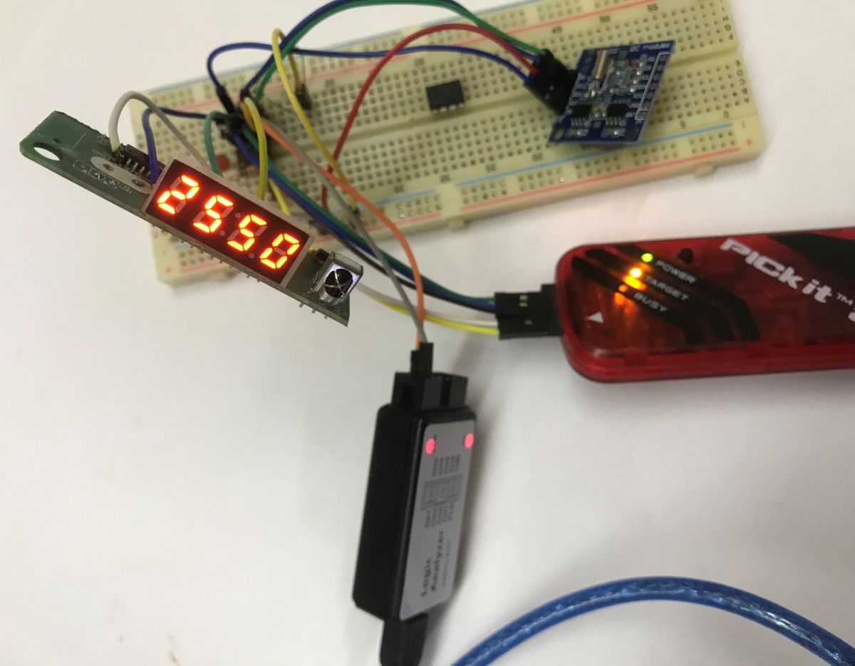
    Simple clock on PIC12F683 - three pins, two I2C buses - DS1307 + FD650
    Simple clock on PIC12F683 - three pins, two I2C buses - DS1307 + FD650 Simple clock on PIC12F683 - three pins, two I2C buses - DS1307 + FD650
    What does it look like under the hood? I have connected a logic analyser to the D0 (clock), D1 (SDA first) and D2 (SDA second) lines. I have added I2C decoders.
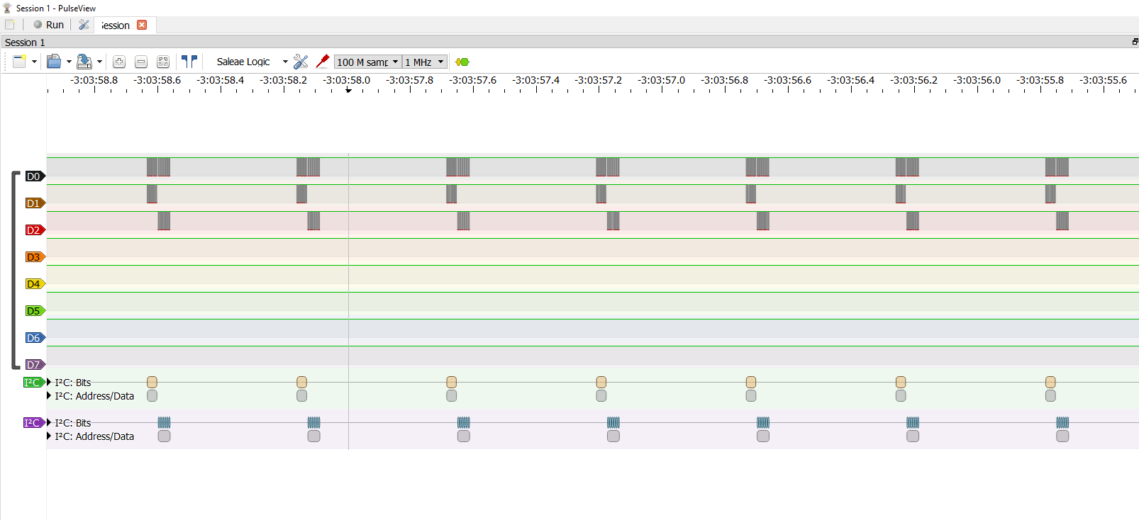
    Simple clock on PIC12F683 - three pins, two I2C buses - DS1307 + FD650
    When zoomed in you can see the correctly decoded transactions. No problems with start/stop conditions, no "ghosts" on the line:
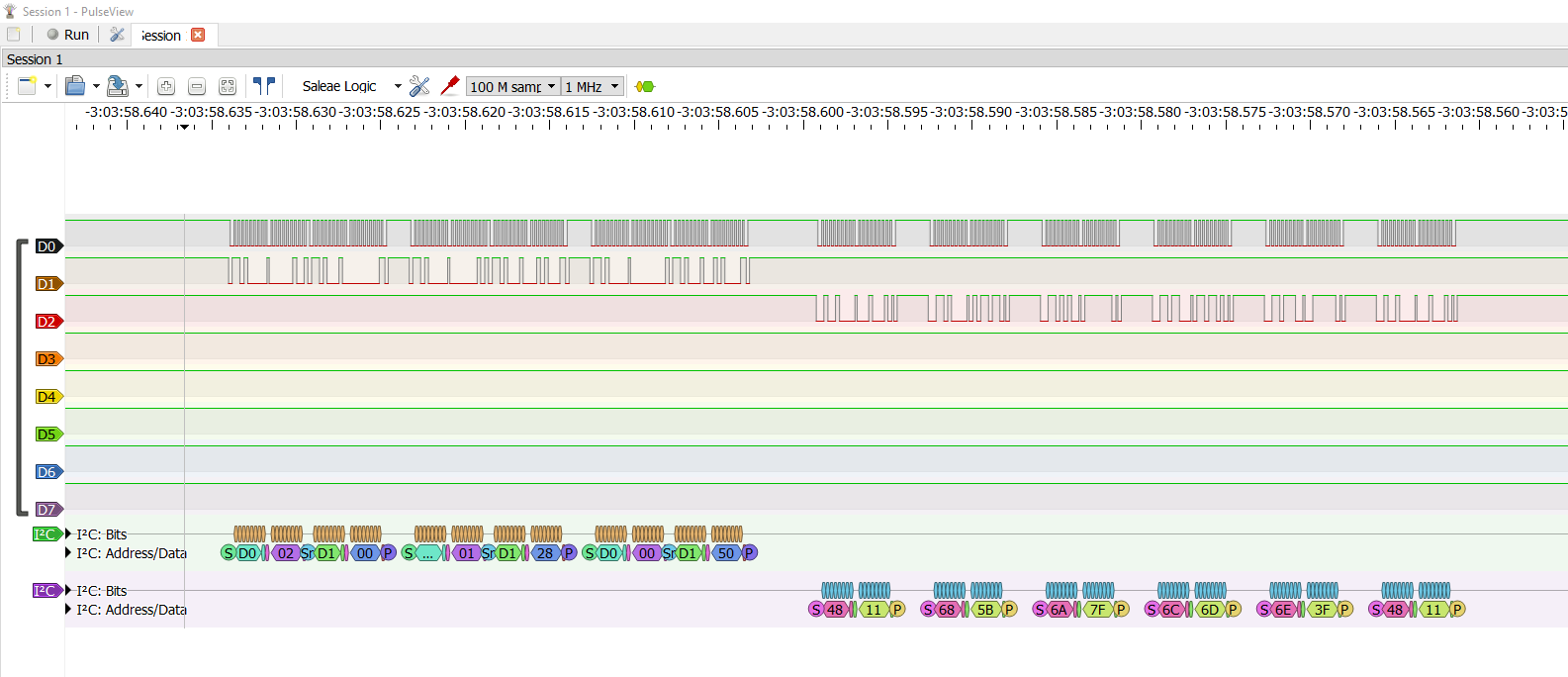
    Simple clock on PIC12F683 - three pins, two I2C buses - DS1307 + FD650
    This is what the time reading from the DS1307 looks like. You can see the characteristic address 0x68 (after shifting and adding the read/write bit 0xD0 or 0xD1) and reading from registers 0, 1, and 2, the value 00:28:50.
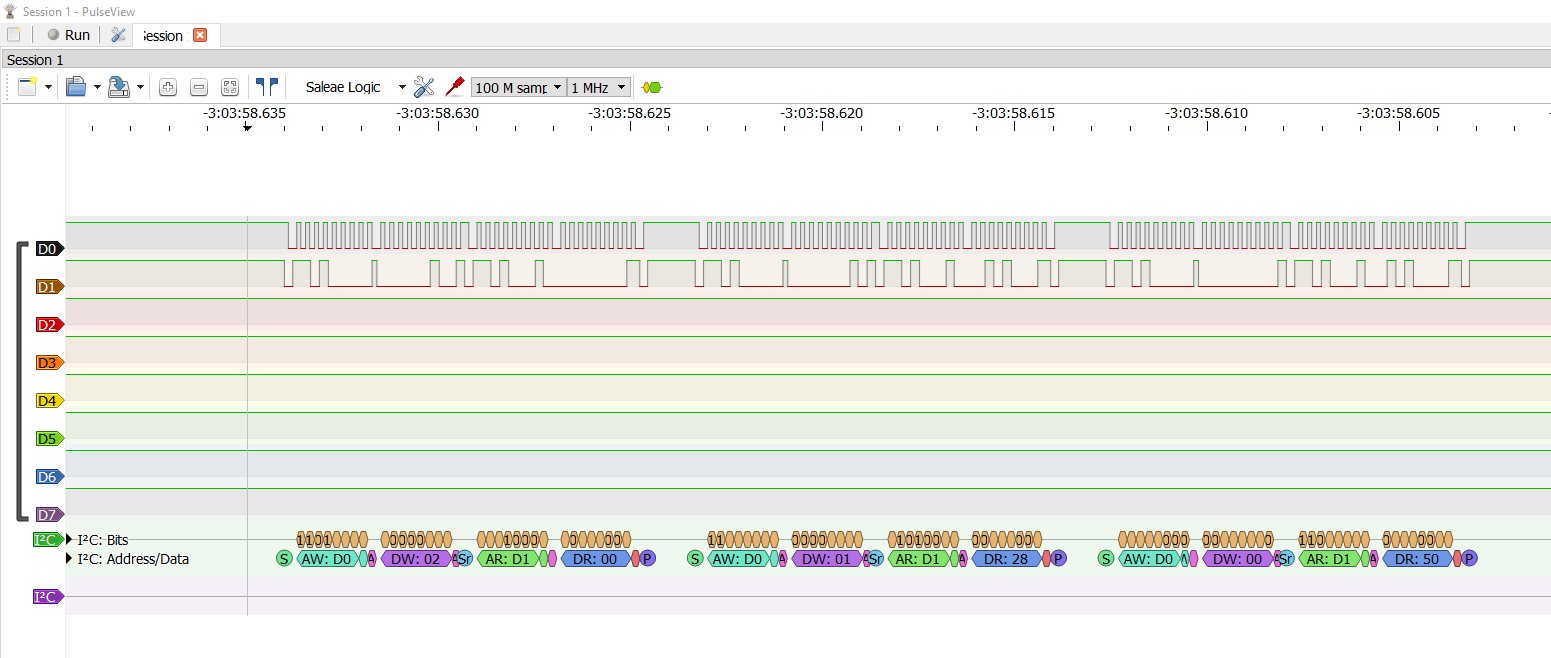
    Simple clock on PIC12F683 - three pins, two I2C buses - DS1307 + FD650
    Similarly, the display control. Here you can see the sent segments of the individual digits.
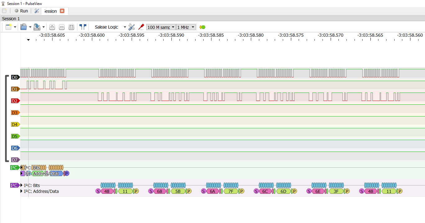
    Simple clock on PIC12F683 - three pins, two I2C buses - DS1307 + FD650

    Key reading
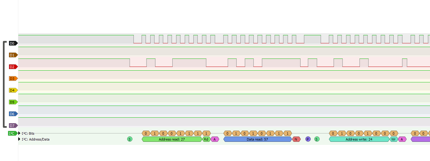
    The next step is to read the keys. I don't have keys on my board, so I added two according to the schematic earlier in the post. I then implemented reading them - reading via I2C from address 0x27. The key code is then returned, as well as a flag as to whether it is/was pressed.
    Code: C / C++
    Log in, to see the code

    As a test, I display this code on the display in hexadecimal format. By the way, I added characters 10-15 to the character map.
    Code: C / C++
    Log in, to see the code

    The reading can be seen on the analyser:
    Simple clock on PIC12F683 - three pins, two I2C buses - DS1307 + FD650
    This makes it easy to identify the codes of the keys you have:


    Limits, everywhere limits
    At this stage the PIC's memory limits began to kick in:
    
    pic12f683_clockI2C.asm:1877:Message[1304] Page selection not needed for this device. No code generated.
    message: Using default linker script "C:\Program Files (x86)\gputils\lkr\12f683_g.lkr".
    warning: Relocation symbol "_cinit" [0x0000] has no section. (pass 0)
    error: No target memory available for section "IDD_idata_0_i".
    error: Error while writing hex file.
    

    I reworked and rewrote the program to put the functions in the main loop where possible and reduce the number of variables.

    Finalize the clock
    The final step is to add the hour and minute setting. These two buttons are sufficient for this. I have assumed that:
    - one just toggles the mode (operation, edit hour, edit minute)
    - the other increases the selected value, a single press increases it once and holding down the key increases it continuously by 1 as long as the key is held
    To do this, I read the keys every loop, examine the current mode (work, edit hour, edit minute), in the case of editing I flash the selected digits and handle the key events accordingly. After editing, the time is saved.
    Code: C / C++
    Log in, to see the code

    Result:


    Case combinations
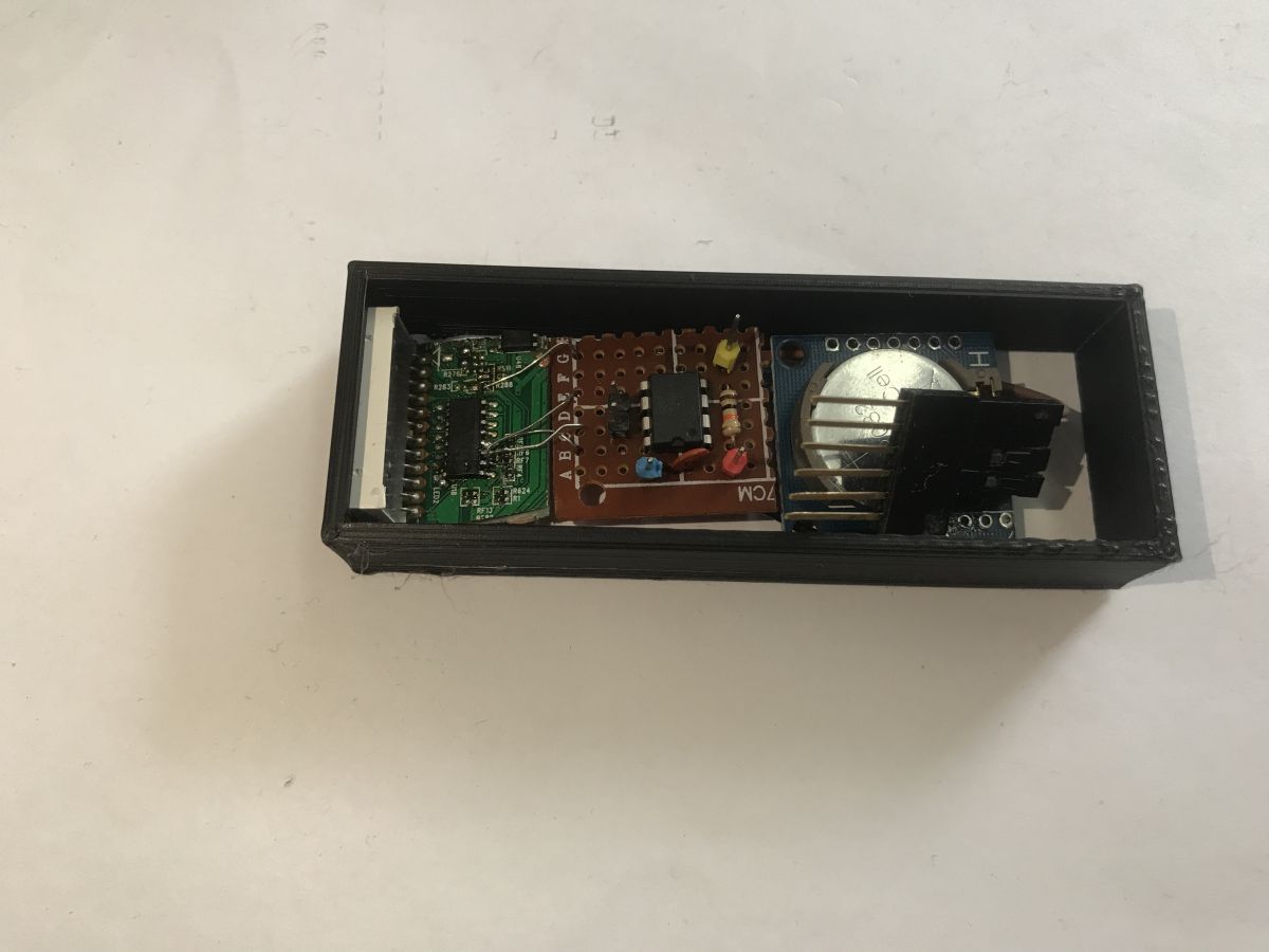
    I have also started making the enclosure, but that will be in a separate topic.
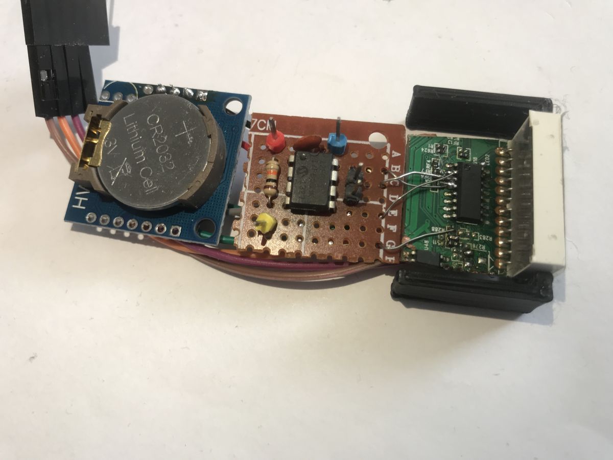
    Simple clock on PIC12F683 - three pins, two I2C buses - DS1307 + FD650
    Simple clock on PIC12F683 - three pins, two I2C buses - DS1307 + FD650


    Summary
    The project proved to be a very interesting and unusual experience. I've run the FD650 before and it wasn't a problem, but here I practiced pin saving (this PIC12F has little free IO, and I may still want to add an alarm soon, an ADC would be useful too) and then general optimisation. In the end, I managed to fit the whole thing on a small PIC and a functional clock came out programmatically.
    Now the hardware can still be worked on - the board shown here could be made smaller, probably by cutting off unnecessary parts of the laminate, and then printing the case on a 3D printer and placing the buttons in a clever way.
    Perhaps I will deal with this in a separate section.
    I am attaching a version of the design for SDCC .
    Attachments:
    • pic12f683_clockI2C.zip (48.54 KB) You must be logged in to download this attachment.

    Cool? Ranking DIY
    Helpful post? Buy me a coffee.
    About Author
    p.kaczmarek2
    Moderator Smart Home
    Offline 
    p.kaczmarek2 wrote 14459 posts with rating 12468, helped 650 times. Been with us since 2014 year.
  • ADVERTISEMENT
  • #2 21891616
    viayner
    Level 43  
    Posts: 10575
    Help: 1557
    Rate: 2009
    Hello,
    i see that you and ekoleg have been discussing PIC based circuits for a while now, are they back in favour?
    These are already old, even very old circuits, but still functional, I have used them myself for a long time, even before the arduino or ATmegs appeared.
    I applaud you for your willingness to optimise, partly due to hardware limitations, but also because of the old school belief that optimising the code is better than reaching for better hardware, as you can see, such a little thing can do the job.
    Best regards
📢 Listen (AI):

FAQ

TL;DR: Ten zegar używa tylko 3 pinów GPIO PIC12F683 i rozdziela magistralę na 2 linie SDA. „FD650 zajmuje wiele adresów”, więc nie może współdzielić standardowej I2C z DS1307. To FAQ pomaga hobbystom elektroniki zbudować mały zegar z RTC, wyświetlaczem 7-seg i programową I2C na bardzo małym PIC-u. [#21891006]

Dlaczego to ważne: Ten projekt pokazuje, jak uruchomić RTC i 4-cyfrowy wyświetlacz na mikrokontrolerze z 128 B RAM, mimo niepełnej zgodności jednego układu z I2C.

Rozwiązanie Linie Zgodność adresowania Efekt w projekcie
Jedna wspólna I2C 1×SDA + 1×SCL FD650 nie zachowuje się jak standardowe urządzenie adresowane Konflikty adresów, błędne ACK
Dwie magistrale danych współdzielące zegar 2×SDA + 1×SCL DS1307 osobno, FD650 osobno Poprawny odczyt RTC i sterowanie wyświetlaczem

Kluczowy wniosek: Najważniejsze oszczędzanie pinów nie polega tu na „upchnięciu wszystkiego na jednej I2C”. Polega na rozdzieleniu problematycznego FD650 od poprawnego DS1307, ale pozostawieniu wspólnej linii SCL, więc cały zegar nadal działa na 3 pinach.

Quick Facts

  • PIC12F683 w projekcie ma 128 B RAM, a cały zegar używa tylko 3 pinów GPIO: GP0, GP1 i GP2. [#21891006]
  • Autor ustawił wewnętrzny oscylator PIC12F683 na 4 MHz (OSCCON = 0b01100001) i generował opóźnienia programowo. [#21891006]
  • FD650 steruje wyświetlaczem 4-cyfrowym przez bajty pod adresami 0x68, 0x6A, 0x6C, 0x6E, a włączenie wyświetlacza następuje przez 0x48 → 0x11. [#21891006]
  • DS1307 jest odczytywany jako RTC po rejestrach 0x00, 0x01, 0x02, a bit 0x80 w rejestrze sekund zatrzymuje licznik czasu. [#21891006]
  • Analizator stanów logicznych pracował z częstotliwością 24 MHz, co pozwoliło potwierdzić poprawne start, stop, ACK i bajty danych na obu liniach SDA. [#21891006]

1. Why does the FD650 need a separate SDA line from the DS1307 instead of sharing one standard I2C bus on the PIC12F683?

FD650 potrzebuje osobnej linii SDA, bo nie zachowuje się jak pełni adresowalne urządzenie I2C. W skanie magistrali odpowiadał na wiele adresów, choć fizycznie był jedynym układem na tej linii. DS1307 działa poprawnie w standardowej I2C, ale FD650 zakłócałby jego adresowanie. Dlatego projekt używa 2 linii danych i 1 wspólnej linii SCL, czyli łącznie 3 pinów GPIO. [#21891006]

2. How do you implement two software I2C buses with a shared SCL pin on a PIC12F683 using only three GPIO pins?

Robisz dwie osobne programowe I2C z własnymi liniami SDA i wspólnym SCL. W projekcie GP0 obsługuje FD650, GP1 obsługuje DS1307, a GP2 jest wspólnym zegarem. 1. Zdefiniuj osobne makra sda_high/low i ds_sda_high/low. 2. Współdziel scl_high i scl_low dla obu zestawów funkcji start, stop, read i write. 3. Używaj osobnych funkcji i2c_* dla wyświetlacza i ds_i2c_* dla RTC, aby nie mieszać ACK i odczytu. [#21891006]

3. What is the FD650, and how is it related to the TM1650 and HD2015 display controllers?

FD650 to sterownik wyświetlacza LED 7-segmentowego, użyty tu do obsługi 4 cyfr i klawiszy. „FD650 jest sterownikiem wyświetlacza, który obsługuje segmenty LED i klawisze, ale nie trzyma się w pełni standardowego adresowania I2C.” W wątku podano, że jest klonem TM1650 i występuje też pod nazwą HD2015. Autor odzyskał taki moduł ze starego tunera DVB i uruchomił go bez dodatkowych rezystorów segmentów. [#21891006]

4. What is the DS1307 RTC, and what does the clock halt bit do in its seconds register?

DS1307 to układ RTC podtrzymujący czas i datę nawet po wyłączeniu mikrokontrolera. „DS1307 RTC jest układem zegara czasu rzeczywistego, który przechowuje czas w rejestrach i może pracować z baterią podtrzymującą, zachowując odmierzanie po zaniku zasilania głównego.” Bit 0x80 w rejestrze sekund to clock halt. Gdy jest ustawiony, licznik czasu stoi. Kod inicjalizacji odczytuje rejestr 0x00 i czyści ten bit przez zapis sec & 0x7F. [#21891006]

5. How can I scan an I2C bus with Arduino to prove that an FD650 responds on multiple addresses?

Wystarczy wysłać na Arduino kolejne adresy od 1 do 126 i sprawdzać ACK po każdym bajcie adresowym. Kod z wątku używał pinów 2 i 3, programowej I2C oraz delayMicroseconds(5). Jeśli FD650 jest sam na magistrali, a skan nadal zwraca wiele aktywnych adresów, masz dowód konfliktu. Autor dodatkowo odłączył jedną linię i pokazał, że komunikacja natychmiast się psuje, co potwierdziło prawdziwe odpowiedzi układu. [#21891006]

6. What segment addresses and data bytes do you send to an FD650 to display a 4-digit time like 12:34?

Najpierw włączasz wyświetlacz komendą 0x48 → 0x11, a potem wysyłasz cztery cyfry pod 0x68, 0x6A, 0x6C i 0x6E. Dla mapy segmentów z wątku liczby 1, 2, 3, 4 to odpowiednio 0x06, 0x5B, 0x4F, 0x66. Dla czasu 12:34 sekwencja to więc 0x68→0x06, 0x6A→0xDB z kropką 0x80, 0x6C→0x4F, 0x6E→0x66. Bez dwukropka drugi bajt wynosi 0x5B. [#21891006]

7. How do you port bit-banged I2C code from Arduino to PIC12F683 in SDCC when working directly with TRISIO and GPIO registers?

Trzeba zastąpić pinMode i digitalWrite bezpośrednią obsługą TRISIO i GPIO. Na Arduino stan wysoki robił się przez INPUT_PULLUP, a na PIC-u przez ustawienie wejścia wysokiej impedancji; stan niski przez wyzerowanie bitu w GPIO i przełączenie pinu na wyjście. Kod SDCC definiuje makra dla GP0, GP1 i GP2 oraz ręcznie generuje start, stop, zapis i odczyt bitów. To zachowuje tę samą logikę, ale działa na rejestrach mikrokontrolera. [#21891006]

8. Why do the PIC12F683 weak pull-ups work for the FD650 and DS1307 in this project without extra external pull-up resistors?

W tym układzie wewnętrzne podciąganie PIC12F683 okazało się wystarczające do stabilnej pracy obu linii SDA i wspólnego SCL. Autor włączył globalne WPU przez OPTION_REG &= 0b01111111 oraz lokalnie ustawił WPU = 0b00000111 dla GP0, GP1 i GP2. Projekt działał bez dodatkowych rezystorów zewnętrznych, a analizator pokazał poprawne start, stop i ACK. To jest fakt z tej konkretnej płytki, nie uniwersalna reguła dla każdej magistrali I2C. [#21891006]

9. How can a logic analyzer help debug start, stop, ACK, and data bytes on the FD650 and DS1307 lines?

Analizator logiczny pozwala zobaczyć, czy programowa I2C naprawdę generuje poprawne przebiegi. Autor podpiął 3 kanały: D0 do SCL, D1 do pierwszej SDA i D2 do drugiej SDA, a potem dodał dekodery I2C. Dzięki temu zweryfikował warunki start i stop, odpowiedzi ACK oraz konkretne bajty, takie jak 0x48, 0x68 czy 0xD0/0xD1. Zrzuty pokazały też brak „ghostów” i poprawny odczyt czasu 00:28:50 z rejestrów DS1307. [#21891006]

10. What does clock stretching mean in I2C, and why does the shared SCL macro wait for the line to go high?

Clock stretching oznacza, że urządzenie podrzędne może chwilowo zatrzymać magistralę, przytrzymując SCL w stanie niskim. „Clock stretching jest mechanizmem I2C, w którym układ podrzędny opóźnia kolejny takt zegara, aby zyskać czas na przygotowanie danych lub ACK.” Dlatego makro scl_high nie tylko zwalnia linię, ale też czeka w pętli while(!READ_SCL);. To chroni transmisję przed sytuacją, w której kod uzna linię za wysoką, choć fizycznie układ jeszcze ją blokuje. [#21891006]

11. FD650 vs DS1307 on the same bus: what protocol behavior causes address conflicts, and how is it different from a fully compliant I2C device?

Konflikt powoduje to, że FD650 nie traktuje pierwszego bajtu jak klasycznego adresu urządzenia I2C. W wątku wyjaśniono, że pierwszy bajt bywa dla niego komendą albo adresem rejestru, więc układ odpowiada na wiele wartości podczas skanu. DS1307 działa inaczej: ma poprawny adres urządzenia 0x68, który po dodaniu bitu R/W daje 0xD0 lub 0xD1. To właśnie różnica między układem zgodnym z I2C a sterownikiem, który tylko częściowo naśladuje tę magistralę. [#21891006]

12. How do you read buttons through the FD650 at address 0x27 and tell a real key press from the last stored key code?

Odczyt klawiszy polega na zapisie adresu odczytu 0x4F, a potem odebraniu jednego bajtu danych z FD650. Jeśli układ nie potwierdzi ACK, funkcja zwraca 0, bo klawisz raczej nie jest wciśnięty. Prawdziwe naciśnięcie rozpoznajesz po bicie 0x40: gdy nie jest ustawiony, bajt zawiera tylko historię ostatniego kodu matrycy. Autor pokazał też test w hexie na dwóch ostatnich cyfrach wyświetlacza, co ułatwia identyfikację kodów przycisków. [#21891006]

13. What is BCD in the DS1307 registers, and how do you convert between BCD and normal binary values for hours, minutes, and seconds?

BCD to format, w którym każda połówka bajtu przechowuje jedną cyfrę dziesiętną. „BCD jest sposobem kodowania liczb dziesiętnych, w którym starszy i młodszy nibble przechowują osobne cyfry 0–9, co upraszcza zapis czasu w rejestrach RTC.” W kodzie konwersja do liczby binarnej to ((val >> 4) * 10) + (val & 0x0F), a odwrotnie ((val / 10) << 4) | (val % 10). Dla sekund trzeba jeszcze maskować bit zatrzymania: sec & 0x7F. [#21891006]

14. Why does a PIC12F683 project hit 'No target memory available for section IDD_idata_0_i', and what code changes help fit the clock into limited RAM?

Ten błąd pojawia się, gdy projekt nie mieści danych inicjalizowanych w bardzo małej pamięci RAM PIC12F683. W tym wątku ograniczenie było realne, bo mikrokontroler ma tylko 128 B RAM, a program rozrósł się po dodaniu RTC, dwóch I2C i obsługi klawiszy. Autor zmniejszył użycie pamięci przez przenoszenie funkcji do pętli głównej, redukcję liczby zmiennych i świadome złamanie zasady DRY, tworząc dwa proste zestawy funkcji I2C zamiast bardziej ogólnej warstwy. [#21891006]

15. How do you add two-button time setting with short press, long press auto-repeat, and blinking edit digits on an FD650 clock driven by a PIC12F683?

Dodajesz prostą maszynę stanów z trzema trybami: zegar, edycja godzin i edycja minut. Jeden przycisk BTN_NEXT = 0x57 przełącza tryb, a drugi BTN_PLUS = 0x4F zwiększa wartość. Krótkie naciśnięcie dodaje +1, a długie używa progów LONG_PRESS_THR = 8 i REPEAT_RATE = 2 do autorepeat. Miganie realizuje licznik g_blinkcnt i flaga F_BLINK_ON; po zakończeniu edycji kod zapisuje czas do DS1307 przez ds1307_set_time(g_h, g_m). [#21891006]
Generated by the language model.
ADVERTISEMENT