FAQ
TL;DR: On the PLG 20 A1, the charge rail is ~21 VDC; "overcharging ... could result in fireworks." This guide helps DIYers repair faults and test continuous output safely on Parkside chargers and converted packs. [Elektroda, olsefb, post #21033992]
Why it matters: It answers how to fix no‑charge faults, identify parts, and understand safe workarounds without bricking packs or chargers.
Quick facts:
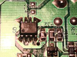
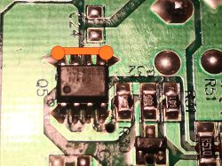
- Output rail engages at approx. 21 VDC via Q5; forcing Q5 on (SO‑8 pins 5–8) ties the pack to the rail. [Elektroda, olsefb, post #21033992]
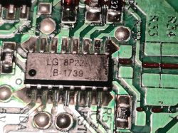
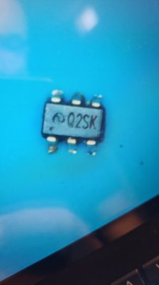
- PWM controller SMD codes Q2SE/Q2SK correspond to LD7536; swapping to LD7536 restored operation. [Elektroda, diogobreis, post #21097303]
- Common input faults: ABS10 bridge and T3.15 A fuse; replacing both revived charging. [Elektroda, jasiek_1953, post #20393509]
- The third pin carries cyclic pulses for pack‑charger comms; simple spoofing is impractical. [Elektroda, kazikszach, post #20016278]
- Charger logic follows a programmed profile (e.g., CC/CV), so off‑label charging can misbehave. [Elektroda, azaghorth, post #20370702]
Quick Facts
- Output rail engages at approx. 21 VDC via Q5; forcing Q5 on (SO‑8 pins 5–8) ties the pack to the rail. [Elektroda, olsefb, post #21033992]
- PWM controller SMD codes Q2SE/Q2SK correspond to LD7536; swapping to LD7536 restored operation. [Elektroda, diogobreis, post #21097303]
- Common input faults: ABS10 bridge and T3.15 A fuse; replacing both revived charging. [Elektroda, jasiek_1953, post #20393509]
- The third pin carries cyclic pulses for pack‑charger comms; simple spoofing is impractical. [Elektroda, kazikszach, post #20016278]
- Charger logic follows a programmed profile (e.g., CC/CV), so off‑label charging can misbehave. [Elektroda, azaghorth, post #20370702]
How do I make a Parkside PLG 20 A1 charge continuously?
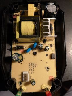
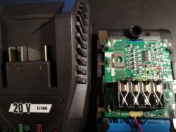
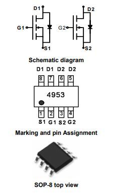
Locate Q5, a dual P‑MOSFET (often 4935/4953). Force it on or short drain–source by bridging SO‑8 pins 5 and 8. This connects the pack directly to the ~21 VDC rail. Monitor voltage, time, and temperature to prevent damage. "Overcharging ... could result in fireworks." [Elektroda, olsefb, post #21033992]
What does the third/middle pin do, and can I spoof it?
The charger and battery exchange a repeating series of pulses over the third pin. Users report this handshake is required and not easily faked with simple resistors or jumpers. Without it, the charger stays in standby. [Elektroda, kazikszach, post #20016278]
Is it safe to charge a converted Ni‑MH‑to‑Li‑ion pack with this charger?
Not recommended. The charger is programmed for specific packs and profiles (e.g., CC/CV). Mismatched chemistry or BMS behavior may result in improper charging. As one expert warned, "A charger should be used for the purpose it was built." [Elektroda, azaghorth, post #20370702]
What PWM driver is labeled Q2SE/Q2SK/QBRG, and what replacement works?
The primary PWM controller marked Q2SE or Q2SK was replaced successfully with an LD7536. After the swap, the unit resumed operation, confirming compatibility. [Elektroda, diogobreis, post #21097303]
Has swapping to an LD7536 actually revived a dead PLG 20 A1?
Yes. One repair report confirms replacing the Q2SE‑coded device with an LD7536 brought the charger back to life and charging worked. [Elektroda, xanderkg, post #19593843]
My series bulb glows at max and the 47 µF/400 V cap reads 0 V—what does that imply?
That pattern points to a primary‑side fault. A user observed full‑bright lamp behavior with 0 V on the bulk capacitor and suspected the power transistor was continuously on. [Elektroda, HackoBoy, post #19257292]
Which input parts commonly fail on this charger?
Check the ABS10 rectifier bridge and the T3.15 A fuse. Replacing a burnt ABS10 and the fuse restored normal operation for one owner, indicating a frequent failure path. [Elektroda, jasiek_1953, post #20393509]
What exactly is Q5 on this charger’s board?
Q5 is a dual P‑channel MOSFET, typically labeled 4935 or 4953. Bridging its SO‑8 pins 5 and 8 connects the battery directly to the ~21 VDC charge rail, bypassing pack detection. [Elektroda, olsefb, post #21033992]
What are Q6 and Q11, and what specs were observed?
They were reported as small‑signal NPN BJTs. Measured characteristics were hFE≈290, Ube≈700 mV, and Ic≈6.2 mA under test conditions. Choose similar parts if replacements are needed. [Elektroda, silerty45, post #21541929]
What is the U2 IC on the PLG 20 A1 board?
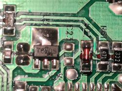
U2, marked “9ARF,” was identified by connections as a TL431‑type reference/error amplifier. This device shapes feedback and regulation in the charger control loop. [Elektroda, silerty45, post #21541929]
Can I use the PLG 20 A1 as a 21 V power source?
For testing, yes—by forcing Q5 on or shorting pins 5–8, the battery sees ~21 VDC continuously. Closely monitor voltage, current, and temperature, and disconnect promptly to avoid pack damage. [Elektroda, olsefb, post #21033992]
How do I force charging for troubleshooting (3‑step)?
- Locate Q5 (dual P‑MOS, 4935/4953) on the board.
- Bridge Q5 SO‑8 pins 5 and 8 to tie the pack to ~21 VDC.
- Watch pack voltage and time; remove the bridge before overcharge risk. [Elektroda, olsefb, post #21033992]