Converting a logic circuit made with AND and OR gates to a form composed of NAND and NOR gates is an excellent exercise that will help you understand the basic laws of Boola logic. The article below is divided into three sections. It is based on the homework of a student who asked for help on the EEWeb forum. The essence of this task is as follows:
* The student was presented with a logical equation.
* He was instructed to create an appropriate truth table.
* He was told to minimize the Karnaugh map.
* Finally needs to create an implementation using only NAND gates or only NOR gates.
Let's start by considering why this kind of problem class should even be considered. Next, we'll look at the specific equation from the problem in more detail, moving on to the initial AND-OR solution. Later we will consider general concepts for transforming AND-OR based circuits into their NAND-NOR counterparts. Finally, we will use what we have learned to answer the final part of the task.
Why is it worth using only NAND gates or only NOR gates?
Why was there a request during the class to implement a logical function using only NAND gates or only NOR gates? While students may be surprised by this, the lecturer is not necessarily a bitter, frustrated person whose only pleasure in life is making their lives difficult. Of course, this cannot be ruled out as a possible motivation, but there is some practical justification for this task.
First, transforming the circuit described using AND and OR gates (in the sum of products or product of sums format) and transforming it into an alternate representation using only NAND gates, only NOR gates, or a mixture of NAND and NOR gates is a great way to make sure that you understand how different logic gates work and you can use DeMorgan's laws.
Second - if you design a printed circuit board (PCB) using single, integrated logic gates, e.g. integrated circuits containing six NOT gates or four 2-input AND, OR, NAND or NOR gates, there may be situations where one is missing. eg AND gates, but there is redundant NAND and NOT gates - in this case, understanding logic gates can eliminate the need to add a new integrated circuit.
The simplest logic gate is NOT. Assuming we're talking about CMOS technology, the NOT gate will require two transistors. Further down the complexity ladder are the NAND and NOR gates, each containing four transistors. Then we have AND and OR gates, each with six transistors. All this means that the use of NAND or NOR gates instead of AND or OR allows the number of transistors in the system to be reduced by up to a third. This is of great importance when implementing logic elements in integrated circuits.
An AND gate is actually made up of a NAND gate followed by a NOT gate (similarly an OR gate consists of a NOR gate followed by a NOT gate). In addition to using more transistors: 4 + 2 = 6 as stated above, this means that the AND gate (and the OR gate) consists of two delay elements (the propagation time is longer). So, converting AND to NAND (and OR to NOR) will make the circuit run faster.
Currently, few circuits are designed at the gate level. Instead, layouts at a high level of abstraction arise; a complex synthesis algorithm is then used to generate the corresponding equivalent at the logic gates level. This means that most of the above points are not as important in professional practice as they used to be, but it is still good to have these skills.
Let us return to our task. The lecturer presented the following equation:
$$D = \bar{A}B\bar{C} + AB\bar{C} + A\bar{B}\bar{C} + \bar{A}\bar{B}C + \bar{A}BC + ABC$$
They can be used to generate the following truth table. The student described above created the following table:
This is where the difficulties probably begin. There are six products in his equation, each of which should have a corresponding 1 in the result column of the truth table, but in the table presented there are only five 1s related to the output.
The basic problem is the lack of understanding of Boolean logic. This causes confusion when constructing this type of table. Each of us has ever started out and was lost in these laws, so let's take some time to follow step by step how to construct a correct truth table for the above issue.
The first thing you need to do is count the individual products in the equation to see where the individual ones are in the scoreboard. Let us number the individual products:
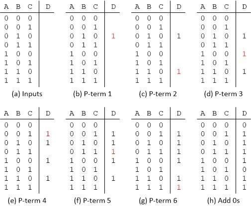
The next step is to create a truth table. We start with all the input combinations shown as a standard binary number as shown in (a) below, then add the six 1s corresponding to the six products as shown in (b) to (g), and finally fill any remaining output fields with zeros as shown in (h) below.
First of all, it should be noted that translating an equation into a truth table is not at all difficult. It is important to appreciate the logic underlying this process. Understanding how to approach the above equation is simple, it essentially says itself: "The output is true (1 on the output) if the first product (first AND function) is true OR if the second product is true OR if the third product is true. the product is true, etc. ". Therefore, we can simply put 1's in the output column corresponding to each of our products - the result will be true (1) if any of these products are true, otherwise the result will be false (0).
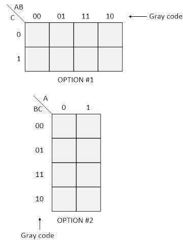
The next step is to create the Karnaugh map. We start by creating the mesh itself. Since we have three inputs, we can do it in two ways as below screenshot shown:
It doesn't matter which option we use. The answer will be the same in both cases. We will use option number one. When looking at map number 1, notice where "AB" is. On the right side there are four combinations of zeros and ones that can be associated with AB inputs: "00", "01", "11" and "10". It is very important to note that these combinations are represented in Gray code which means that only one bit changes as we move from one value to the next. This is the key to the operation of the Karnaugh map.
In natural binary code, when we go from 01 to 10, two bits change. For comparison, if we look at the corresponding shift in the Gray code (01 to 11), only one bit changes.
In addition, consider the last line of the binary code. If we were to wrap around and go from this line to the first line (11 to 00), then - again - two bits change. However, if we look at the corresponding lines in the Gray code (10 to 00) we see that - again - only one bit changes.
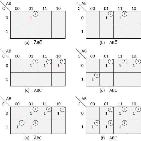
Now let's complete the Karnaugh map. We do this by adding 1 to each square that corresponds to the product in our equation. We will do this step by step again as shown below (the little numbers from 1 to 6 in circles correspond to the products in our original equation):
It should also be noted that we do not need a truth table to complete the Karnaugh map. It is enough if we go through our equation and for each product we add 1 to the corresponding area of the Karnaugh map.
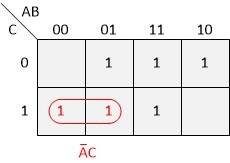
The next step is to use our Karnaugh map to minimize the layout. Looking at the final Karnaugh (f) map above, we immediately see that we can reduce it to just three terms. As always, let's do it step by step.
The two 1s highlighted in the image below mean that the result in both cases is 1. For each of these fields, A = 0 and C = 1, so these values are valid, B = 0 for one of these fields and 1 for the other field. This means that as long as A = 0 and C = 1, it does not matter whether B is 0 or 1.
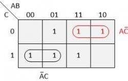
Then let's look at the second group of two ones highlighted in the image below. For each of these fields, A = 1 and C = 0, so these values are valid. Again, B = 0 for one of these fields and 1 for the other. This says that as long as A = 1 and C = 0, it does not matter what state line B takes.
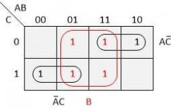
Finally, let's look at the group of four ones highlighted in the image below. One of the tricks with Karnaugh maps is that we can use the same ones as part of multiple groups.
In this case, the value of variables A and C does not matter - the only variable that has the same value for these ones is B and it is always one. This means that the minimization result from the Karnaugh map looks like this:
$$D = \bar{A}B + A\bar{C} + B$$
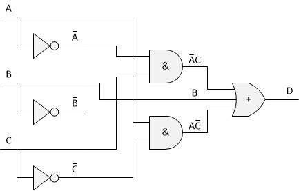
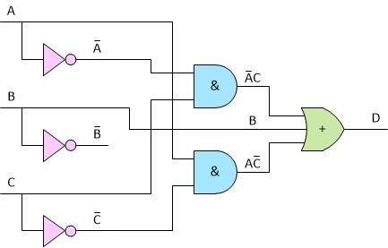
From here, we can easily draw a circuit diagram with logic gates using the NOT, AND and OR gates. The diagram corresponding to this equation is shown below:
Before you notice - we know that we are not using the! B signal (the! Sign means negation, and this notation means NOT B). We will use it in the future, however, so let it stay on the diagram. Speaking of the future, the next step is to implement the last part of the task and use only NAND or NOR gates.
But we will be using it in the near future. This future is closer than you think. This is the point where we need to put our thinking caps on as it was the job of the disgusting lecturer to represent the final circuit using only NAND gates or only NOR gates.
Implementing NOT gates using NAND or NOR
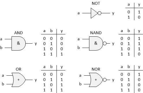
Let's start with the simplest, which in this case means three NOT gates. First, let's recall the truth tables for the five popular goals. They are shown below:
This means that if we connect both inputs of a NAND gate together, the result will be a functional equivalent of a NOT gate. The same situation applies to NOR gates with connected both inputs.
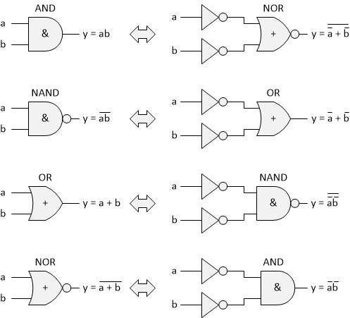
DeMorgan transformations on AND, OR, NAND and NOR gates
Augustus DeMorgan (1806-1871) was a contemporary of George Bool. DeMorgan made a significant contribution to the field of symbolic logic. First of all, he developed a set of rules that we now call DeMorgan transformations.
To perform a DeMorgan transformation on a logic equation, we perform the following steps:
1. Replace all AND operators with OR operators and vice versa.
2. Invert all input variables; also replace any zeros with ones and vice versa.
3. Invert the entire function.
4. Reduce multiple inversions.
Carrying out such a transformation is of course possible on single gates. The result of such an operation is as follows:
Representing our circuit using only NAND gates
In the above part, we will find the foundations for our final task - reducing the system to the NAND gates only. Let's recall what a circuit we play in looks like when it is implemented with NOT, AND and OR gates:
The gates are color coded to make it clear what will happen next step by step. Suppose we want to use only NAND gates. So, using everything explained so far, let's convert the NOT, OR and AND gates to NAND gates.
Let's start with the three NOT gates shown in pink to the left. We can replace each of these gates with a 2 input NAND gate with the inputs connected so no problems.
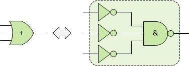
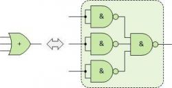
Next, let's take a look at the three-input OR gate, marked in green. It is on the right side of our diagram. According to the DeMorgan transform, we know that we can replace it with a three-input NAND gate by adding NOT gates at the inputs as shown below.
Again, as before, we can convert each of the three added NOT gates into a NAND gate as shown below.
Now we just need to worry about the two AND gates, marked blue in the center of the circuit. Obviously, the DeMorgan transformations are not helpful here, since the equivalent of an AND gate is a NOR gate with NOT gates at the inputs, and we assumed that we cannot use NOR gates in this exercise.
Fortunately, this has a simple solution, we just have to remember that the AND gate is really made up of a NAND gate followed by a NOT gate (similarly an OR gate consists of a NOR gate followed by a NOT gate). This means we can replace the selected AND gates as shown below:
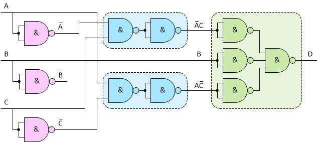
Of course, once again, we need to change the NOT gates to their equivalent, made of NAND gates, as we only want to use this kind of logic gates in our system. The layout after the transformation looks like this:
Now we are almost to the end. Let's see what our layout looks like after putting together all the transformations we've done so far:
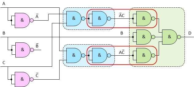
Functionally, this system will perform the function entrusted to it, however, it is far from optimal. We can see that in two cases there is another NOT gate after the NOT gate (both implemented with NAND gates, of course). Both cases are marked in the figure below with a red outline.
Each even number of negations connected in series gives the output exactly the same state as the input (plus the delay, but this is not important in these considerations). So we can just turn them into a simple connection.
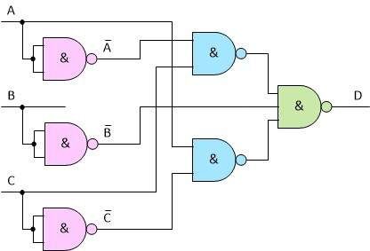
After all optimizations, the layout looks as follows:
As we wrote in the introduction - the systems are transformed into a form with NAND gates to speed up their operation. Let's look at it in the example above. Suppose the NOT, NAND, and NOR gates each have a delay of one and the AND and OR gates are two.
In the first, original design, the worst-case delay is 1 + 2 + 2 = 5, and for comparison, in the case of the diagram above, the propagation time will be 1 + 1 + 1 = 3, which is 40% less.
If you are a student and you are still waiting for Boola algebra classes, then familiarize yourself with the above article - the information contained in it will certainly be useful. The DeMorgan transformation issues and the minimization of the Karnaugh tables are at the core of this subject.
Source: https://www.eeweb.com/profile/max-maxfield/ar...-logic-functions-using-only-nand-or-nor-gates
* The student was presented with a logical equation.
* He was instructed to create an appropriate truth table.
* He was told to minimize the Karnaugh map.
* Finally needs to create an implementation using only NAND gates or only NOR gates.
Let's start by considering why this kind of problem class should even be considered. Next, we'll look at the specific equation from the problem in more detail, moving on to the initial AND-OR solution. Later we will consider general concepts for transforming AND-OR based circuits into their NAND-NOR counterparts. Finally, we will use what we have learned to answer the final part of the task.
Why is it worth using only NAND gates or only NOR gates?
Why was there a request during the class to implement a logical function using only NAND gates or only NOR gates? While students may be surprised by this, the lecturer is not necessarily a bitter, frustrated person whose only pleasure in life is making their lives difficult. Of course, this cannot be ruled out as a possible motivation, but there is some practical justification for this task.
First, transforming the circuit described using AND and OR gates (in the sum of products or product of sums format) and transforming it into an alternate representation using only NAND gates, only NOR gates, or a mixture of NAND and NOR gates is a great way to make sure that you understand how different logic gates work and you can use DeMorgan's laws.
Second - if you design a printed circuit board (PCB) using single, integrated logic gates, e.g. integrated circuits containing six NOT gates or four 2-input AND, OR, NAND or NOR gates, there may be situations where one is missing. eg AND gates, but there is redundant NAND and NOT gates - in this case, understanding logic gates can eliminate the need to add a new integrated circuit.
The simplest logic gate is NOT. Assuming we're talking about CMOS technology, the NOT gate will require two transistors. Further down the complexity ladder are the NAND and NOR gates, each containing four transistors. Then we have AND and OR gates, each with six transistors. All this means that the use of NAND or NOR gates instead of AND or OR allows the number of transistors in the system to be reduced by up to a third. This is of great importance when implementing logic elements in integrated circuits.
An AND gate is actually made up of a NAND gate followed by a NOT gate (similarly an OR gate consists of a NOR gate followed by a NOT gate). In addition to using more transistors: 4 + 2 = 6 as stated above, this means that the AND gate (and the OR gate) consists of two delay elements (the propagation time is longer). So, converting AND to NAND (and OR to NOR) will make the circuit run faster.
Currently, few circuits are designed at the gate level. Instead, layouts at a high level of abstraction arise; a complex synthesis algorithm is then used to generate the corresponding equivalent at the logic gates level. This means that most of the above points are not as important in professional practice as they used to be, but it is still good to have these skills.
Let us return to our task. The lecturer presented the following equation:
$$D = \bar{A}B\bar{C} + AB\bar{C} + A\bar{B}\bar{C} + \bar{A}\bar{B}C + \bar{A}BC + ABC$$
They can be used to generate the following truth table. The student described above created the following table:
AND | B | C. | D |
0 | 0 | 0 | 0 |
0 | 0 | 1 | 0 |
0 | 1 | 0 | 1 |
0 | 1 | 1 | 1 |
1 | 0 | 0 | 1 |
1 | 0 | 1 | 0 |
1 | 1 | 0 | 1 |
1 | 1 | 1 | 1 |
This is where the difficulties probably begin. There are six products in his equation, each of which should have a corresponding 1 in the result column of the truth table, but in the table presented there are only five 1s related to the output.
The basic problem is the lack of understanding of Boolean logic. This causes confusion when constructing this type of table. Each of us has ever started out and was lost in these laws, so let's take some time to follow step by step how to construct a correct truth table for the above issue.
The first thing you need to do is count the individual products in the equation to see where the individual ones are in the scoreboard. Let us number the individual products:
The next step is to create a truth table. We start with all the input combinations shown as a standard binary number as shown in (a) below, then add the six 1s corresponding to the six products as shown in (b) to (g), and finally fill any remaining output fields with zeros as shown in (h) below.
First of all, it should be noted that translating an equation into a truth table is not at all difficult. It is important to appreciate the logic underlying this process. Understanding how to approach the above equation is simple, it essentially says itself: "The output is true (1 on the output) if the first product (first AND function) is true OR if the second product is true OR if the third product is true. the product is true, etc. ". Therefore, we can simply put 1's in the output column corresponding to each of our products - the result will be true (1) if any of these products are true, otherwise the result will be false (0).
The next step is to create the Karnaugh map. We start by creating the mesh itself. Since we have three inputs, we can do it in two ways as below screenshot shown:
It doesn't matter which option we use. The answer will be the same in both cases. We will use option number one. When looking at map number 1, notice where "AB" is. On the right side there are four combinations of zeros and ones that can be associated with AB inputs: "00", "01", "11" and "10". It is very important to note that these combinations are represented in Gray code which means that only one bit changes as we move from one value to the next. This is the key to the operation of the Karnaugh map.
Natural binary code | Gray code |
00 | 00 |
01 | 01 |
10 | 11 |
11 | 10 |
In natural binary code, when we go from 01 to 10, two bits change. For comparison, if we look at the corresponding shift in the Gray code (01 to 11), only one bit changes.
In addition, consider the last line of the binary code. If we were to wrap around and go from this line to the first line (11 to 00), then - again - two bits change. However, if we look at the corresponding lines in the Gray code (10 to 00) we see that - again - only one bit changes.
Now let's complete the Karnaugh map. We do this by adding 1 to each square that corresponds to the product in our equation. We will do this step by step again as shown below (the little numbers from 1 to 6 in circles correspond to the products in our original equation):
It should also be noted that we do not need a truth table to complete the Karnaugh map. It is enough if we go through our equation and for each product we add 1 to the corresponding area of the Karnaugh map.
The next step is to use our Karnaugh map to minimize the layout. Looking at the final Karnaugh (f) map above, we immediately see that we can reduce it to just three terms. As always, let's do it step by step.
The two 1s highlighted in the image below mean that the result in both cases is 1. For each of these fields, A = 0 and C = 1, so these values are valid, B = 0 for one of these fields and 1 for the other field. This means that as long as A = 0 and C = 1, it does not matter whether B is 0 or 1.
Then let's look at the second group of two ones highlighted in the image below. For each of these fields, A = 1 and C = 0, so these values are valid. Again, B = 0 for one of these fields and 1 for the other. This says that as long as A = 1 and C = 0, it does not matter what state line B takes.
Finally, let's look at the group of four ones highlighted in the image below. One of the tricks with Karnaugh maps is that we can use the same ones as part of multiple groups.
In this case, the value of variables A and C does not matter - the only variable that has the same value for these ones is B and it is always one. This means that the minimization result from the Karnaugh map looks like this:
$$D = \bar{A}B + A\bar{C} + B$$
From here, we can easily draw a circuit diagram with logic gates using the NOT, AND and OR gates. The diagram corresponding to this equation is shown below:
Before you notice - we know that we are not using the! B signal (the! Sign means negation, and this notation means NOT B). We will use it in the future, however, so let it stay on the diagram. Speaking of the future, the next step is to implement the last part of the task and use only NAND or NOR gates.
But we will be using it in the near future. This future is closer than you think. This is the point where we need to put our thinking caps on as it was the job of the disgusting lecturer to represent the final circuit using only NAND gates or only NOR gates.
Implementing NOT gates using NAND or NOR
Let's start with the simplest, which in this case means three NOT gates. First, let's recall the truth tables for the five popular goals. They are shown below:
This means that if we connect both inputs of a NAND gate together, the result will be a functional equivalent of a NOT gate. The same situation applies to NOR gates with connected both inputs.
DeMorgan transformations on AND, OR, NAND and NOR gates
Augustus DeMorgan (1806-1871) was a contemporary of George Bool. DeMorgan made a significant contribution to the field of symbolic logic. First of all, he developed a set of rules that we now call DeMorgan transformations.
To perform a DeMorgan transformation on a logic equation, we perform the following steps:
1. Replace all AND operators with OR operators and vice versa.
2. Invert all input variables; also replace any zeros with ones and vice versa.
3. Invert the entire function.
4. Reduce multiple inversions.
Carrying out such a transformation is of course possible on single gates. The result of such an operation is as follows:
Representing our circuit using only NAND gates
In the above part, we will find the foundations for our final task - reducing the system to the NAND gates only. Let's recall what a circuit we play in looks like when it is implemented with NOT, AND and OR gates:
The gates are color coded to make it clear what will happen next step by step. Suppose we want to use only NAND gates. So, using everything explained so far, let's convert the NOT, OR and AND gates to NAND gates.
Let's start with the three NOT gates shown in pink to the left. We can replace each of these gates with a 2 input NAND gate with the inputs connected so no problems.
Next, let's take a look at the three-input OR gate, marked in green. It is on the right side of our diagram. According to the DeMorgan transform, we know that we can replace it with a three-input NAND gate by adding NOT gates at the inputs as shown below.
Again, as before, we can convert each of the three added NOT gates into a NAND gate as shown below.
Now we just need to worry about the two AND gates, marked blue in the center of the circuit. Obviously, the DeMorgan transformations are not helpful here, since the equivalent of an AND gate is a NOR gate with NOT gates at the inputs, and we assumed that we cannot use NOR gates in this exercise.
Fortunately, this has a simple solution, we just have to remember that the AND gate is really made up of a NAND gate followed by a NOT gate (similarly an OR gate consists of a NOR gate followed by a NOT gate). This means we can replace the selected AND gates as shown below:
Of course, once again, we need to change the NOT gates to their equivalent, made of NAND gates, as we only want to use this kind of logic gates in our system. The layout after the transformation looks like this:
Now we are almost to the end. Let's see what our layout looks like after putting together all the transformations we've done so far:
Functionally, this system will perform the function entrusted to it, however, it is far from optimal. We can see that in two cases there is another NOT gate after the NOT gate (both implemented with NAND gates, of course). Both cases are marked in the figure below with a red outline.
Each even number of negations connected in series gives the output exactly the same state as the input (plus the delay, but this is not important in these considerations). So we can just turn them into a simple connection.
After all optimizations, the layout looks as follows:
As we wrote in the introduction - the systems are transformed into a form with NAND gates to speed up their operation. Let's look at it in the example above. Suppose the NOT, NAND, and NOR gates each have a delay of one and the AND and OR gates are two.
In the first, original design, the worst-case delay is 1 + 2 + 2 = 5, and for comparison, in the case of the diagram above, the propagation time will be 1 + 1 + 1 = 3, which is 40% less.
If you are a student and you are still waiting for Boola algebra classes, then familiarize yourself with the above article - the information contained in it will certainly be useful. The DeMorgan transformation issues and the minimization of the Karnaugh tables are at the core of this subject.
Source: https://www.eeweb.com/profile/max-maxfield/ar...-logic-functions-using-only-nand-or-nor-gates
Cool? Ranking DIY