I recently received a message from Kalesh Sasidharan, the founder behind the Sciotronics project, who asked me to share his solution with the community. And honestly—why not? It’s a clever idea, and the Kickstarter campaign has already proven it’s got real interest behind it.
The motivation behind the project is a familiar pain: prototyping with SMD components can be a real headache. Traditional breadboards don’t support them directly, and while adapters exist, they quickly lead to a messy tangle—especially when you need to tweak your design. Ordering a new PCB for every little change? That gets expensive and slow, fast.
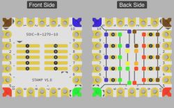
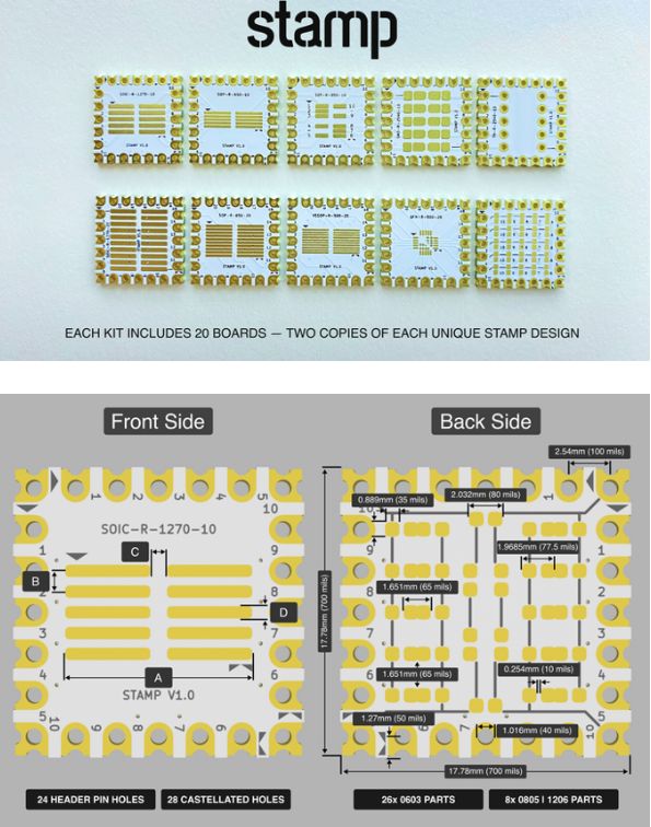
Stamp aims to fix that. It’s a set of reusable breakout boards with pre-defined footprints for the most common SMD components. The main chip goes on the front, and supporting components (resistors, caps, etc.) fit on the back. And despite its compact size—just 17.8 × 17.8 mm—each board can host full circuits: buck converters, sensor modules, even microcontrollers.
What really makes the Stamp system stand out are the clever design touches. Each board has semi-circular edge holes so you can connect multiple boards—either side-by-side or at right angles. It’s a modular, flexible, and reusable approach to prototyping. Think of it like a breadboard for SMD components—only more compact and clean.
The creators highlight three common frustrations with traditional prototyping:
• Only through-hole components: Breadboards just don’t support SMD natively.
• Tangled and error-prone setups: Adapters + flying wires = problems.
• Slow progress: Waiting weeks for every small PCB revision.
With Stamp, you get:
• Built-in connections to VCC or GND—no extra wiring required.
• Front/back layout: Main chips on the front, passive components on the rear.
• Free pads for extra components like LEDs or filter caps.
How it works:
• Front side: Your main component (IC, regulator, small QFN, etc.)
• Rear side: Passive elements and GND/VCC routes
• Internal routing: Built-in connections between layers
• Flexible pads: Add what you need—without extra wires
And for expanding horizontally?
• Selective connectivity: Default ‘open’ edges prevent shorts
• Easy linking: Just align and solder the edges
• Quick disconnects: Boards can be joined or separated as needed
Want proof it works? They squeezed an entire 5V buck converter (11 components!) onto a single SOIC-10 Stamp board:
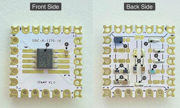
You can build in multiple directions:
• Edge-to-edge: Soldered castellated holes for flat chains
• Right angle/3D: Use pins or connectors for vertical builds
• Jumper pins or 0Ω resistors: Replace solder bridges with real components
⸻
Why Stamp is Worth Checking Out
1. Start building circuits in minutes—with easy tweaks
2. Built-in VCC/GND pads make it intuitive
3. One board = over 27 components
4. Modular = less clutter
5. High-quality PCBs with ENIG gold finish
6. Meets pro standards for trace width, design
7. Easily replace sub-circuits without redoing everything
8. Upgrade parts on the fly
9. Environmentally friendly (no throwaway PCBs)
10. Save time and money during prototyping
11. Compatible with Arduino, Raspberry Pi, etc.
12. Great for making your own shields/modules
⸻
About Sciotronics
Sciotronics is a UK-based startup founded by Dr. Kalesh Sasidharan, who brings a background in systems biology, biomedical electronics, and software. Their mission? Make prototyping faster, more efficient, and accessible.
They launched the project on Kickstarter with a symbolic goal of just PLN840—more about engaging with DIYers and engineers than making money. The initial production run is now done, and kits are shipping. Even better: Stamp is fully open source, with all docs, schematics, and KiCad files available to the community for ongoing improvement.
⸻
Kickstarter:
https://www.kickstarter.com/projects/sciotron...-modular-breakout-boards-for-easy-prototyping
Articles about Stamp:
EEVblog: https://www.youtube.com/watch?v=Xfs0dglIVOM&t=765s
Hackaday: https://hackaday.com/2025/05/28/stamp-modular-breakout-boards-for-smd-prototyping
Hackster.io: https://www.hackster.io/news/sciotronics-stam...ain-out-of-surface-mount-devices-31eb0e0238e8
Project website:
https://sciotronics.com
Also reviewed by a well-known blogger:
Cool? Ranking DIY


