 .
.
How does the shift register work? How can shift registers be cascaded so that you can run 48 LEDs using just two lines - clock and data? Here I will try to demonstrate this using an example of a junk board, which I will also analyse first.
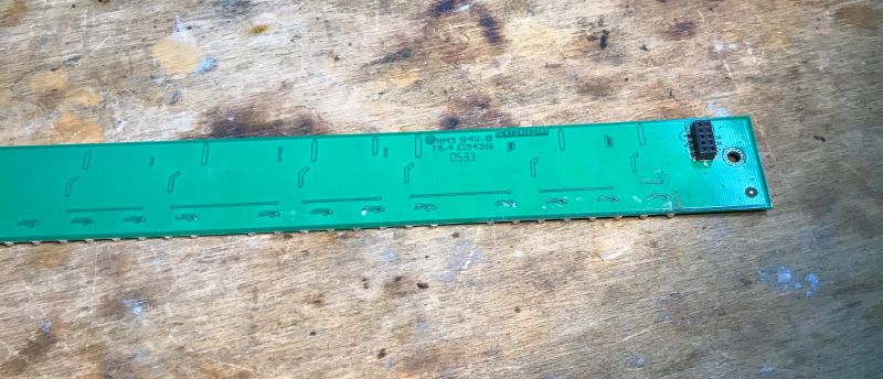
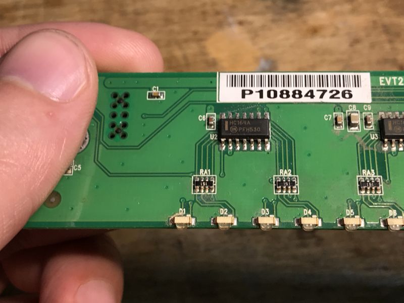
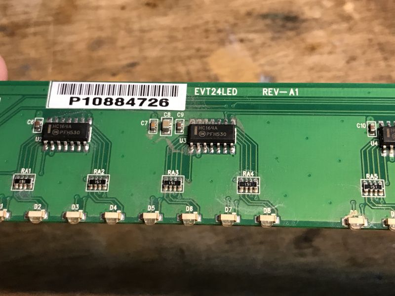
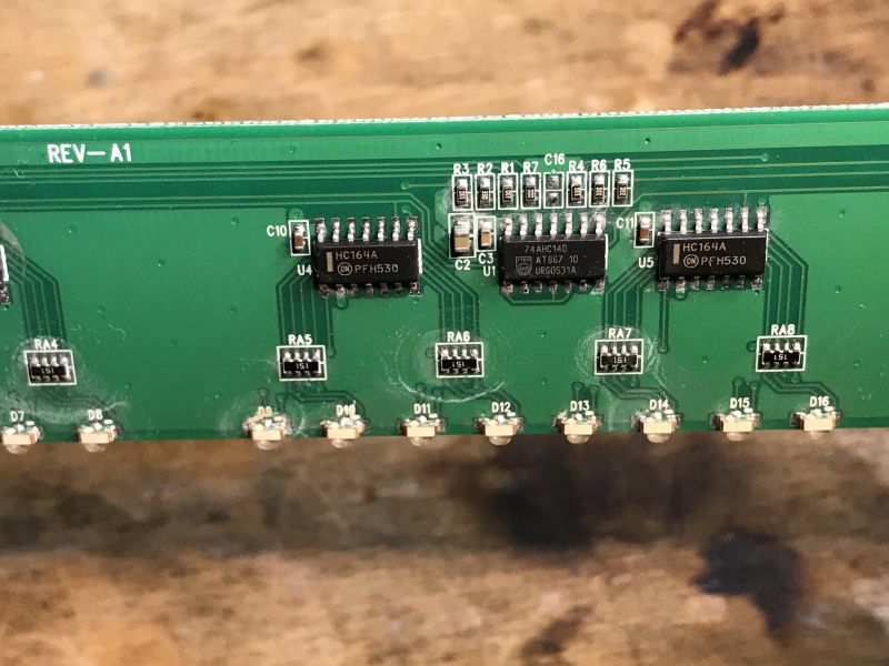
The scouting begins. There are six HC164A chips on the board and one 74AHC14D:
 .
.
 .
.
 .
.
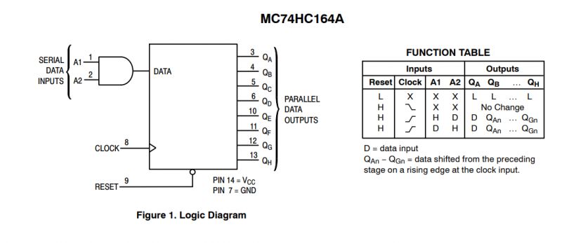
Check the circuit notes, HC164A :
 .
.
The first is a shift register. Input in series, outputs in parallel.
 .
.
This shift register has 8 outputs and only 3 inputs. By feeding the right signal to the inputs, we can set the outputs as we wish, so it essentially allows us to get more IO pins.
The shift register remembers what we set it once.
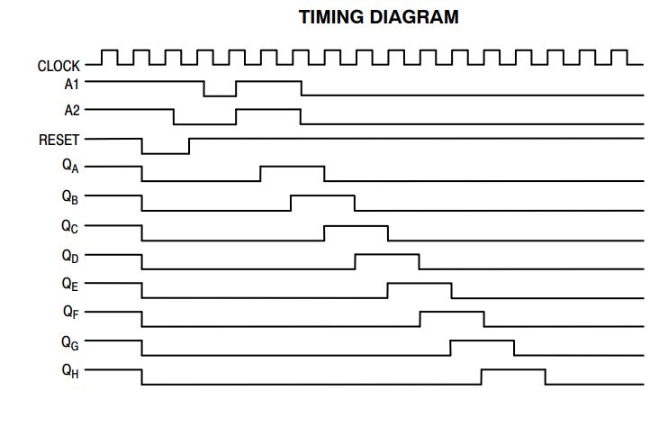
To set its outputs, we feed it a clock signal (CLK), the rising edge of the clock causes the remembered values in the register to move a place further. At this point, the next value is taken (to the first place), which is the result of the logical product of the inputs A1 and A2.
In a simplified application, A2 can be set to high, in which case only A1 and the clock (CLK) are manipulated, and in this way data is written to the next register output pins.
The clock simply executes successive cycles (we set it to low level, then to high level, etc.), and on A1 we put out at our discretion the value we want to write to the location (1 or 0).
This will be a little clearer in the code.
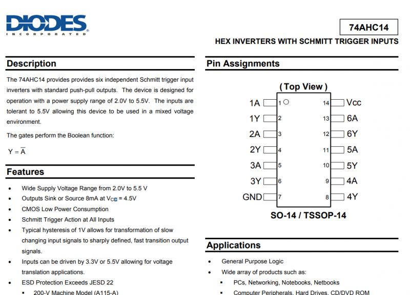
The second circuit is just the gates implementing the NOT function:
 .
.
There are several of these gates inside it, each outputting the opposite logical state to that on the input:
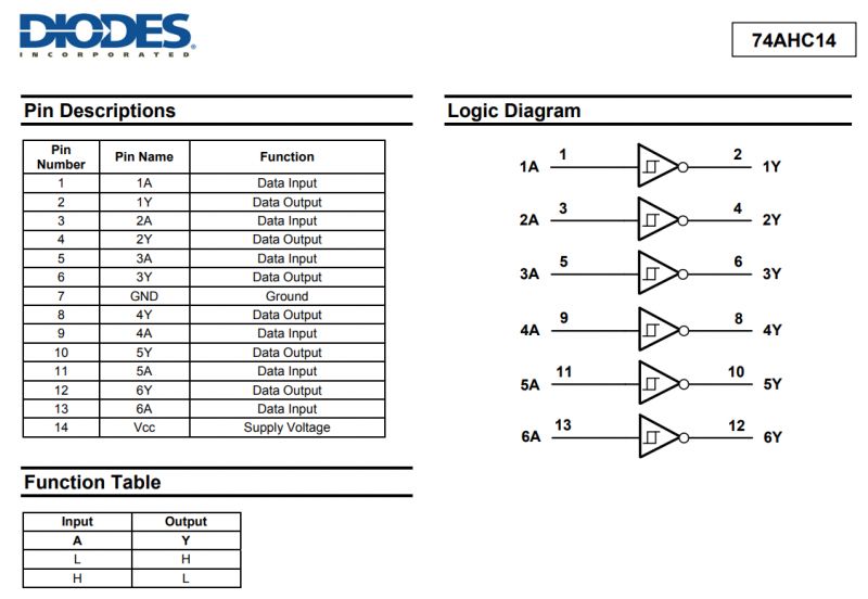 .
.
Now the lead pins need to be examined.
I have desoldered the connector:
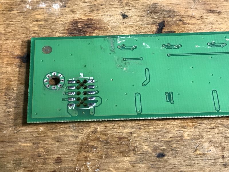 .
.
VDD and GND are the easiest to determine - we have the circuit leads after all. In addition, GND is usually a copper spout on the board, the power supply can often be such a spout too.
We set the multimeter to the continuity test ("beeper") and examine where each pad leads, if by any chance it goes to one of the circuit pins marked VDD or GND in the datasheet.
This leaves only 3 signals, the connection of which I have also examined with a multimeter, putting my observations in the photo:
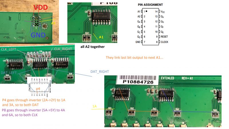 .
.
The conclusions are as follows, we have three signals here:
- a common CLK - this leads to the 74AHC14D, which is in the role of a buffer, and then forks to the combined common clock inputs of the circuits on the right and left side
- common A2 - like the clock, this leads to the 74AHC14D, which is in a buffer role, and then bifurcates
- cascaded A1 - this leads to A1 of the first shift register
Subsequent A1 pins are connected to the QH outputs of the previous shift registers, so that when we sequentially 'insert' bits then the last bit that is 'out' is not lost, it just goes to the next register.
What we have here is essentially a done "one long shift register" built up from several regular registers.
There is still the question of why the NOT gate - we could probably do without it too, I suspect it is only there as a buffer so that there is sufficient current capacity to drive the register inputs. Anyway, these signals go through it twice, so they are not negated afterwards (negation negates negation)..
Startup [/size] .
So we get the Arduino ready, solder the wires:
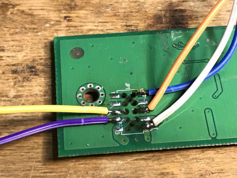 .
.
We take another look at the register's catalogue note to know what to send:
 .
.
Let's make things simpler for ourselves - we'll set this additional common input permanently to a high state. We will only operate the clock and the data entry pin.
We enter our pins in the code as we have connected them:
Code: C / C++
We set them as digital outputs, ENA permanently on high state:
Code: C / C++
And now the most important thing - sending data.
Code: C / C++
For now, I'm sending a 32-bit number, in this case -1, which in bit representation is 0xFFFFFFFFFFFF, which is the lit bits themselves, and then I'm sending the lit bits themselves. I want something to blink.
Apparently something is working, but why alternate?
And I already know, because, after all, those LEDs there are two colours.... so there's a total of 24*2 = 48 bits there, and I'm only sending 32 bits. Additionally, I don't reset anything, so basically I send bits [0,31] first, then [32, 47] and again [0, 15], and so it loops....
I was too hasty in making that first attempt, but I already know what's wrong.
This is now the second attempt. 48 bits is maybe 6 bytes, so I made an array. It was also a bit tempting to use a 64-bit type, but the array will come in handy for demonstration. Now I'm specifically sending 48 bits, so I reckon each new transaction will write a new separate queue of LED states.
Code: C / C++
Still need to test this - one LED for now:
Code: C / C++
Testing:
It works!
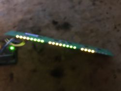
Time for a more ambitious test. I have determined experimentally that the colours of the LEDs alternate....
Code: C / C++
I now light the four LEDs in sequence according to their colour:
It is now left to add support for the individual LEDs.... The bits should be in sequence, you just need to add their setting. Remember this is an array:
Code: C / C++
Demo code:
Code: C / C++
Effect:
And that's it... now you can play around, display some device states, etc, because on the "knight rider" here I would not be tempted because of the "ghosting", about that shortly.
Summary .
It all worked, although I initially thought there would be 24 LEDs here rather than 48, only later did I realise that would be absurd.... We have 6 registers, 8 bits each, so it comes out to 48 bits in total.
Other than that it went smoothly.
The registers are connected in cascade but from a code point of view we don't even have to remember that, they automatically behave as one big register.
I guess the only major problem here is that this particular register doesn't have an "output enable" switch to turn the outputs on/off, so when we "slip" bits into it, for a very short period of time the states are visible on the wrong LEDs. This spoils the effect of the animation and requires additional work to make it look good.
An example of a shift register with such a function could be the 74HC595, in its case it is easier to avoid potential 'ghosting' of segments.
Now the only question is, what to use this module for? Maybe some kind of indicator, but what about "ghosting"? .
PS: This was no longer our first run-in with such a register, I was already running a 7-segment display based on it:
Tuner 7-segment display, running from Arduino, sliding register .
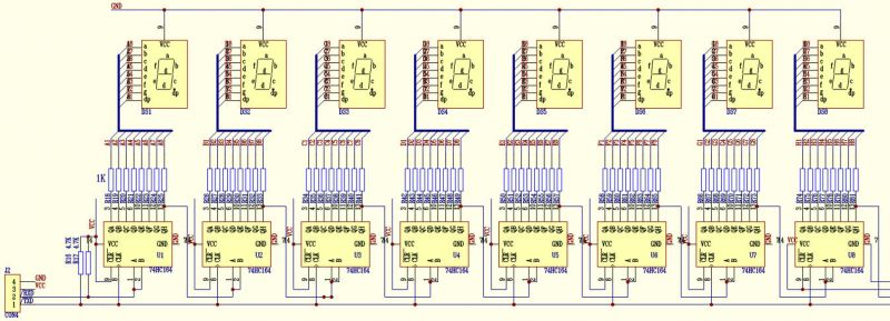
EDIT: There will probably be questions about the schematic, so I found something fitting on the web:
 .
.
Except that in my case all the "B's" are together and I feed a high state to them.
Source: https://www.amobbs.com/thread-3278926-1-1.html
Cool? Ranking DIY Helpful post? Buy me a coffee.


