logo elektroda
logo elektroda
X

What SMD component was on burned trace between FET and diode in Cisco C1000 PSU HR1203?

fuxxy 180 3
ADVERTISEMENT
  • #1 21725466
    fuxxy
    Level 7  
     Cisco C1000 network switch, dead, nothing happens when plugged in.
    This board was initially loaded with corrosion. I removed the bigger components and cleaned off all the corrosion. I'm sure this was the root cause, so I havent tested anything yet.

    This board uses an HR1203 (datasheet) (eval board)to control what appears to be the initial step-down from mains voltage. I've followed the traces, and this implementation is quite similar to the example schematic.

    DatasheetEval Board


    [url=https://obrazki.elektroda.pl/2874595800_1760905442.png][/url]

    Electronic schematic with marked circuit break near diode D3 and transistor Q1


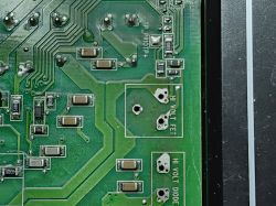
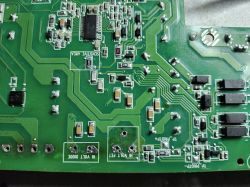
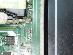
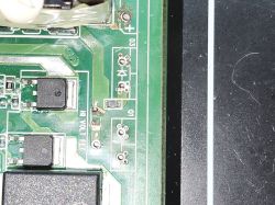
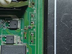
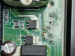
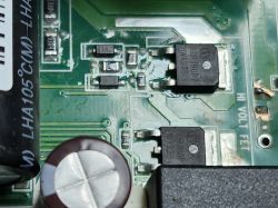
    The burned-out trace in between the FET and the high-power diode appears to have once contained some SMD component.
    I'm trying to figure out what this component may have been, and if it's safe to bypass. The example circuit in the datasheet does not show any components in that signal path.
    Spoiler:
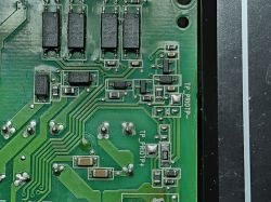
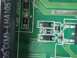
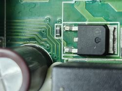
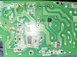
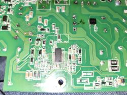
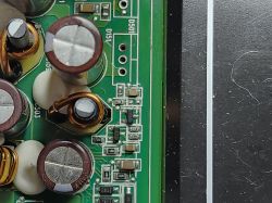
       Close-up of green PCB with labels “HI VOLT FET” and “HI VOLT DIODE” Section of green PCB with SMD electronic components and labels TP_PRIOTP+ and TP_PRIOTP- Close-up of electronic components on a green printed circuit board (PCB). Close-up of electronic components on a green printed circuit board Close-up of a green PCB with visible traces and surface-mounted electronic components.
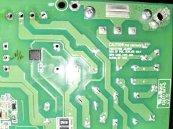
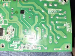
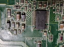
    Green PCB with visible traces, SMD components, and mounting holes Green PCB with visible solder joints, circuit traces, and a fuse warning message Close-up of a green circuit board with visible traces and electronic components. Close-up of a green PCB with ICs and a marked SENSITIVE AREA zone Close-up of a PCB with MPS2438 integrated circuit and surface-mounted components.
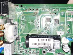
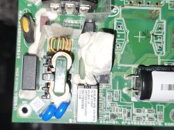
    Printed circuit board with electronic components and visible capacitor PCB power supply module with coils, capacitors, and Chinese label markings Close-up of a damaged transformer on a green PCB Section of green PCB with D3, Q1 labels and surface-mounted electronic components Close-up of a PCB with missing D3 diode and Q1 transistor
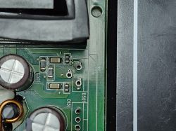
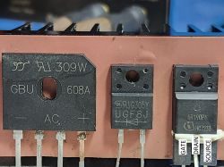
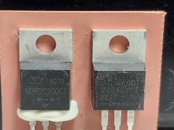
    [url=https://obrazki.elektroda.pl/4207542400_1760904686.jpg][/url] Close-up of a PCB with capacitors and SMD components Section of green printed circuit board with capacitors and SMD components Close-up of damaged green PCB with electronic components and missing elements Close-up of three electronic components mounted on a copper heatsink Two TO-220 semiconductor components on a PCB with visible markings and metal tabs.
    Close-up of printed circuit board with transistors, capacitor, and HI VOLT FET label
  • ADVERTISEMENT
  • #2 21725905
    Telo
    Service technician RTV
    Any photos of the area as this element looked?
    Was anything damaged, any components?
  • ADVERTISEMENT
  • #3 21725917
    Christophorus
    Level 5  
    >>21725466 Any 0-10 ohm protection resistor?
  • #4 21733391
    tevedidat
    Level 2  
    That missing part between the FET and D3 was likely a current-sense resistor or low-value fuse link; it’s there for protection.
    Don’t bypass it directly; check the HR1203 eval schematic for the resistor’s rated value before bridging or replacing it.
ADVERTISEMENT