Power Supply Design Notes: Comparing Different Efficiencies of Devices
TL;DR
- A static power-supply comparison pits a 2N3055 BJT, IRF530 MOSFET, IXYH82N120C3 IGBT, and UF3SC065007K4S SiC MOSFET against the same resistive load.
- Each stage uses an 80 V supply and 15 Ω load, with the BJT driven by base current and the MOSFETs/IGBT driven by gate voltage.
- Measured efficiencies reached 96.54% for the transistor, 99.51% for the Si MOSFET, 98.68% for the IGBT, and 99.93% for the SiC MOSFET.
- The SiC MOSFET delivered the best performance, with only 0.3 W dissipation and 9.9 mΩ channel resistance.
- Designers still need worst-case testing, because reliability, safety, and both static and dynamic losses strongly affect final power-supply efficiency.
This tutorial illustrates several simulations of power circuits driving resistive loads with different devices. Its purpose is is to find out which electronic switch, given the same power supply voltage and load impedance, is the most efficient.
Switching devices over the years
Electronic switches have come a long way over the years and have gotten more powerful. Their evolution concerns various factors such as:
• Resistance of the conduction channel
• Ever-lower costs
• Ever-higher switching speed
• Reduction of the occupied space and less overall dimensions
• Higher efficiency
These are extremely important characteristics, which allow having applications that weren’t imaginable 30 years ago. Initially, the bipolar transistor was the only real power switch. It requires a high base current to conduct, has very slow shutdown characteristics, and is affected by problematic thermal drift. MOSFETs became popular, as they are controlled in voltage and not in current. MOSFETs are not affected by thermal drift and switching losses are lower. For this reason, it was the most used component in power converters. IGBTs took over in the 1980s. An IGBT is a hybrid component between the bipolar transistor and the MOSFET. It has the conduction characteristics of a bipolar transistor, but it is voltage-controlled like a MOSFET. IGBTs are affected by thermal drift, which can be reduced with an additional electrical circuit. Nowadays, SiC and GaN MOSFETs are the new electronic switches and are characterized by exceptional performance. IGBTs handle voltages of 5,000 V and currents of 1,000 A, but the maximum switching frequency does not exceed 100 kHz. MOSFETs work well in high frequency, but the on-resistance is relatively high. These problems are overcome with SiC devices. We will not go into technical details, but we will carry out some simple simulations in a static regime to calculate the efficiency of each individual element.
Efficiency
In the world of power electronics, efficiency is an easy term to conceptualize: 100% is a great value, 0% is bad. Efficient use of energy is a key factor in many applications. Efficiencies above 90% are considered good results, but modern devices allow even higher efficiencies. An efficient power supply obtains less energy waste in the form of heat, which reduces the average life of the electronic components. Efficiency has a great effect on the reliability and durability of the final equipment, as well as on energy consumption. If efficiency is higher, power dissipation and thermal losses are lower. In very high-power converters, even a small percentage of efficiency improvement translates into enormous energy savings and, therefore, economic savings. Furthermore, the higher the efficiency, the lower the operating temperature of the passive and active components and the better the overall reliability of the system. Efficiency is calculated as the output power divided by the input power and is usually expressed as a percentage. The difference between input power and output power is the wasted and lost power in the power supply in the form of heat. The basic formula for calculating the efficiency of a circuit is:

The lower this resistance of the conduction channel of the device, the greater the efficiency of the circuit. In this way, the electronic component will dissipate less heat and will work better.
Electronic components used
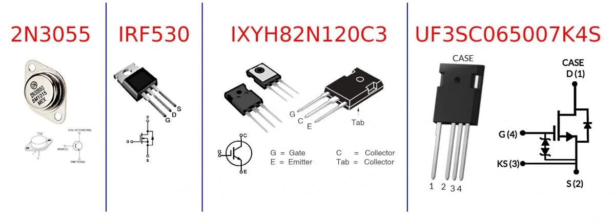
For our tests and simulations, we have chosen some very powerful and robust electronic components (see Figure 1), real workhorses used massively in power projects and which are still widely used today. The following list also describes the most important characteristics:
• Transistor BJT 2N3055: VCE: 100 V, IC: 7 A, P: 115 W, Tj: 200°C, beta: 70
• MOSFET Si IRF530: VDS: 100 V, Rds(on): 0.18 Ω, Id: 14 A, P: 75 W, Tj: 150°C
• IGBT IXYH82N120C3: VCE: 1200 V, VGE: 20 V, IC: 200 A, P: 1250 W, Tj: 175°C
• SiC MOSFET UF3SC065007K4S: VDS: 650 V, Rds(on): 0.009 Ω, VGS: 20 V, Id: 120 A, P: 789 W, Tj: 175°C

Figure 1: Electronic devices used for the efficiency test
Simulations
Figure 2 shows the application scheme for the four electronic devices. These are four equivalent electronic switches that bring the semiconductor components to saturation, driving a fairly robust load. The general characteristics concern the static operation of the load, with the following features:
• Power supply voltage: 80 V
• Resistive load: 15 Ω
• Expected current: 5.3 A approx

Figure 2: Wiring diagram of the four electronic switches
Let’s examine the wiring diagram, which practically consists of four different sections. The first section uses a silicon power transistor. The base must be suitably polarized to be able to make a current equal to that of the base multiplied by the amplification factor (beta) flow on the collector. The base, therefore, is driven in current. The second section includes a silicon MOSFET, and to bring it into conduction, an adequate VGS voltage is required. The third section involves the use of an IGBT, while the fourth section uses a SiC MOSFET. To determine the real efficiency, the powers generated by all energy generators must also be included in the formulas. The four formulas, therefore, are the following. For the transistor stage:

For the silicon MOSFET stage:

For the IGBT stage:

For the SiC FET stage:

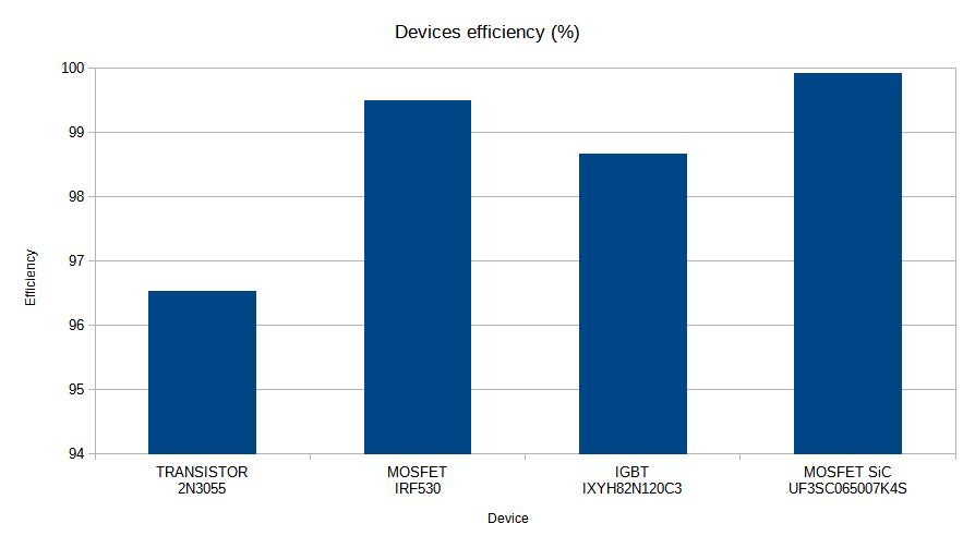
The efficiencies of the four circuits are as follows:
• Transistor: 96.54%
• Si MOSFET: 99.51%
• IGBT: 98.68%
• SiC MOSFET: 99.93%
• It is interesting to observe the power dissipation of each device in full operation:
• Transistor: 3.7 W
• Si MOSFET: 2.1 W
• IGBT: 5.5 W
• SiC MOSFET: only 0.3 W
and the equivalent resistance of the collector-emitter or drain-source channel, calculated with the formula:

• Transistor: 116.4 mΩ
• Si MOSFET: 74.6 mΩ
• IGBT: 200.5 mΩ
• MOSFET SiC: 9.9 mΩ

Figure 3: Graph of the efficiencies of the four devices
A SPICE simulation includes the following directives for the calculation of efficiency:
.meas TRAN Effic1 AVG (abs(V(N001,N005)*I(R2)))/((abs(V(N001)*I(V3)))+(abs(V(N009)*I(V4))))*100
.meas TRAN Effic2 AVG abs(V(N002,N006)*I(R4))/abs(V(N002)*I(V5))*100
.meas TRAN Effic3 AVG abs(V(N003,N007)*I(R1))/abs(V(N003)*I(V1))*100
.meas TRAN Effic4 AVG abs(V(N004,N008)*I(R5))/abs(V(N004)*I(V7))*100
The first solution with the transistor contains the calculation of the power of the two energy sources (base and collector). For the other three simulations, the calculation of the energy on the gate is not necessary, as the generated power is extremely low, being that the MOSFETs are driven in voltage.
Conclusion
When designing a power supply, reliability and safety must be taken into account. Designers need to carefully review the data provided and run lots of tests to calculate worst-use efficiency. The calculation of power losses (static and dynamic) is an obligatory step for the design of power circuits. The techniques for improving the switching system and increasing the efficiency in the circuits are many, and each type of power device has its own characteristics and its own pros and cons, depending on the application (see the graph in Figure 4).

Figure 4: Current graph with an input voltage sweep


Comments