Silicon carbide and gallium nitride power devices have seen increasing usage in some key, high-growth applications in recent years. GaN is now used in mobile device chargers and charging systems. Companies like Apple, Samsung and Xiaomi have chosen GaN-based chargers that provide high power densities while maintaining, or even decreasing, the weight of these components. These chargers utilize power GaN high-electron–mobility transistor (HEMT) chips offered by companies like EPC, GaN Systems and Navitas Semiconductor.
On the other hand, SiC devices have primarily been used in the field of electric mobility. In 2017, electric-vehicle manufacturers like Tesla chose to use SiC-based motor controllers, which boosted the efficiency of their systems. High-volume production of SiC power devices from leading device manufacturers like STMicroelectronics, Infineon Technologies, Wolfspeed and Rohm Semiconductor is now serving the accelerating needs in e-mobility power conversion.
So what is so special about these new semiconductor materials, and why are they being looked at as alternatives to silicon?
As explained by Victor Veliadis, executive director and CTO of
PowerAmerica, in his July 28, 2022, PSMA webinar, “SiC Power Technology Status and Barriers to Overcome”: “SiC and GaN materials have a critical electric field that is about 10× higher than that of silicon, with a bandgap that is 3× higher. In a semiconductor system, the drift layer is what holds its rated voltage, which makes the thickness and doping levels of this layer determine the voltage capability of the device.”
As a result of their thinner, more highly doped drift layers for a given specific on-state resistance and breakdown-voltage specification, SiC devices are smaller in size than silicon, which decreases their capacitances. These devices can therefore efficiently switch at frequencies much higher than what is possible with silicon. Due to the higher switching frequency, the size of passive components and magnetic devices like inductors also decreases. This leads to a significant reduction in the overall size of the system, which increases its power density. Furthermore, the high thermal conductivity allows for high-temperature operation with simplified cooling management, further decreasing system weight and volume.
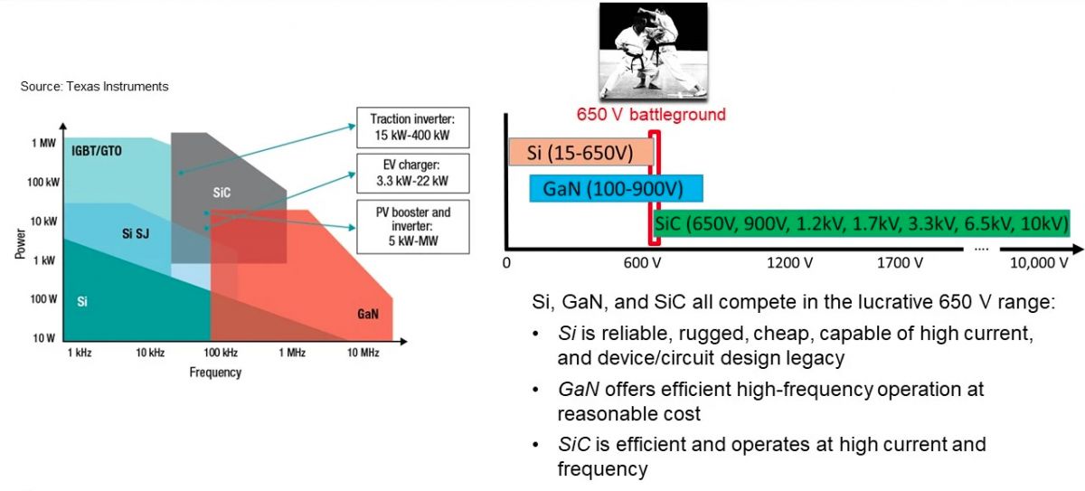
Silicon is still a strong contender in devices rated from 15 V to 650 V while being much cheaper and more reliable, whereas GaN has been gaining popularity in low-power applications like mobile chargers and similar charging systems. As previously mentioned, GaN is the only viable wide-bandgap alternative to silicon in low-power applications, as relative advantages of SiC over Si decrease at voltages below 650 V, especially when the higher cost of SiC is taken into consideration.
GaN & SiC
The zero-reverse–recovery charge in the unipolar GaN HEMT device enables a power-factor–correction (PFC) technology known as “totem-pole bridgeless PFC topology.” These topologies can have advantages of high efficiency at high switching rates.
Stephen Russell, subject matter expert for power devices at Tech Insights, said during a company webinar, “Gallium nitride has truly found its killer app in replacing silicon and USB-C chargers for mobile devices. 2021 [was] a watershed year in market acceptance, and we only expect this momentum to continue. Gallium nitride’s real advantage, however, is its switching: It is the only viable wide-bandgap replacement for silicon at voltages less than 600 V.”
All of these devices compete heavily at the 650-V capacity, which is important, as these devices are used in the 400-V capacity bus for EVs.
 Si, SiC and GaN application space (Source: Victor Veliadis)
SiC is suitable for higher-power applications than what is possible using GaN and is available in voltages ranging from 650 V to 3.3 kV, with higher-voltage devices being developed. It is expected to have an edge in the EV sector, as more and more manufacturers are moving toward 800-V EV systems due to its efficient high-voltage operational capability. Manufacturers like Porsche, Audi, BYD and Hyundai are already working on 800-V battery systems, while Lucid has a 900-V system under development. As Veliadis said, “Moving to 800 V while keeping the current the same doubles the power, with smaller losses. This reduces heavy copper cables, bringing lighter weight and space-saving advantages.”
Challenges in widespread adoption of SiC and GaN
Currently, SiC devices can cost almost 2× to 3× as much as silicon.
Apart from the high cost, manufacturing SiC has its own set of challenges, such as the presence of defects and slower fabrication times compared with silicon. Most SiC manufacturing is on 6-inch manufacturing lines, though 200-mm pilot line efforts have started at some companies like Wolfspeed. Efforts are also being put in at process improvements and better screening capability to improve yield and reliability.
Due to their high-voltage potential, SiC devices are excellent candidates for deployment in power applications like HVDC transmission and renewable-energy systems. For example, in the case of photovoltaic applications, although the SiC device cost is 3× higher than that of silicon, the overall system cost is lower due to the reduction in the size of the passive elements.
There are also projections showing that the SiC market is expected to be worth $6.5 billion by 2027. GaN devices will dominate the low-power mobile application industry, with more devices expected to reach the market with power densities higher than 20 W/in.3. These devices are expected to bring significant efficiency improvements and offer user convenience.
Economies-of-scale cost reductions in both SiC and GaN will create similar positive feedback, as was seen with silicon a couple of decades ago.
Questions
When do you think SiC and GaN power devices will get closer to silicon prices?
Will GaN find a space in EV power-conversion applications where SiC is dominating?
This
article was originally published on sister site Power Electronics News.


Comments