GaN 65W power supply/charger bought for four quid from Aliexpress - tests, thermal imaging, user ris
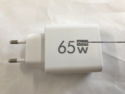
I invite you to test the boisterously advertised welcome gadget offered to us by AliExpress for just £4 with free shipping. Here I will check what performance this power supply has in practice, whether it really supports QC and reaches 65 watts, and whether the voltage at its output is safe for our mobile devices. In addition, I will also look at its PCB under thermal imaging to determine what heats up the most.
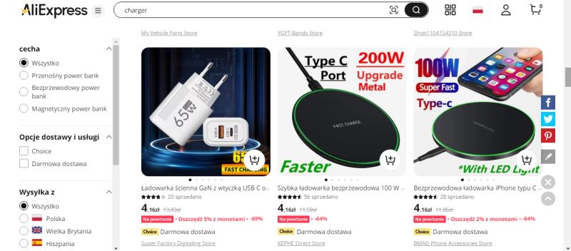
Let's start with the purchase. The whole thing comes under different names, to me it popped up as a "GaN wall charger with USB C plug". I already have reservations about the name itself, if only because essentially the charging circuitry is already in the phone, and here we have, as it already is, a power supply, although I'm more concerned about that GaN and 65 W....

Fast charging (QC standard - higher voltage?) also caught the title. Well, hard, we buy:

If problems arise, simply open discussions with the seller.
First impression First impression
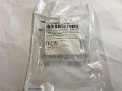
I waited a long time for the package to arrive, but here it is - there's no mistaking it, it says 65W on the packaging and case too:

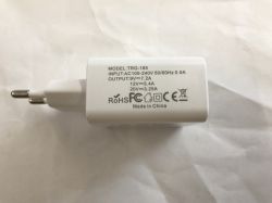
On the device we have its performance (?) - up to 7.2 A at 9 V, up to 5.4 A at 12 V and up to 3.25 A at 20 V:
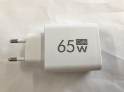

All nice, but QC trigger can't even switch on 7V - what's up?

Let's not judge in advance. The QC trigger may have broken down for me, perhaps it's run-of-the-mill. Worse, at 5 volts I can also draw up to 2 amps and then the voltage drops:


One might get the impression that we have a 5 V 2 A power supply here, but this remains to be checked.
Interior of the gadget
The whole thing is suspiciously easy to disassemble. I can get the impression that this device does the autodisassembly itself when plugged in and pulled harder at an angle.
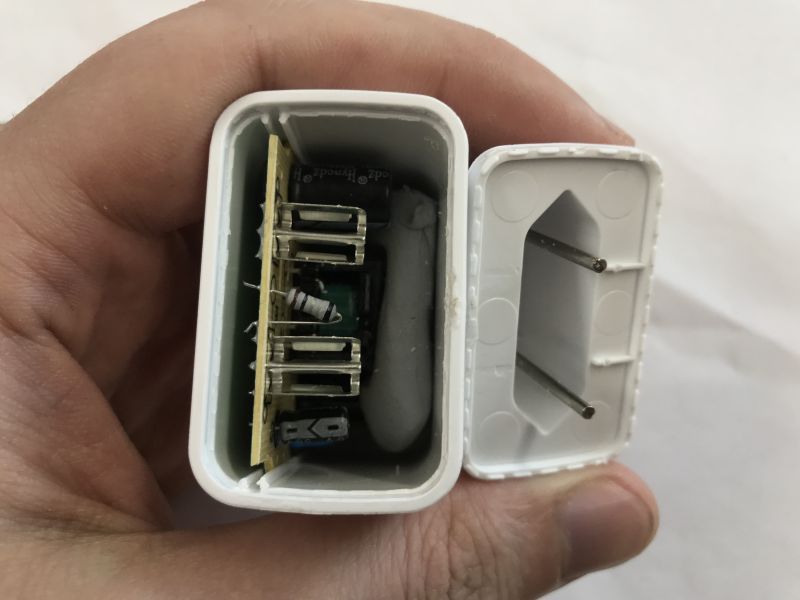
This is how the plug is connected to the board - on contact. Inside we have a small PCB with a load bonus:
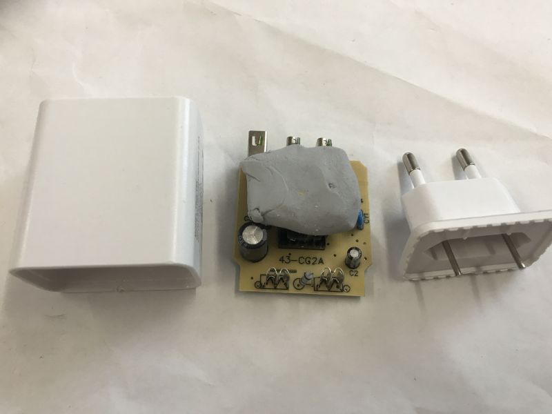
Here's the PCB itself. Everything is on a poor, single-sided board. It does not resemble a GaN power supply:
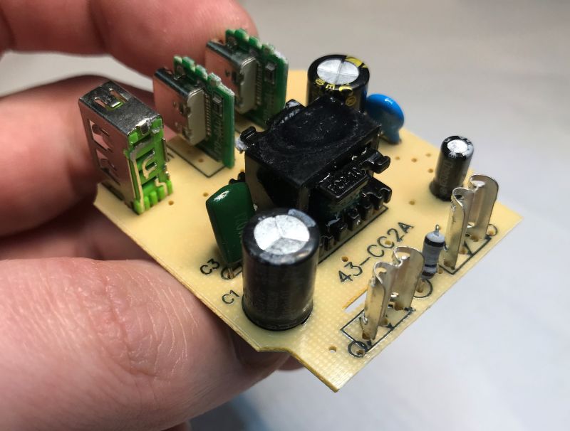
You can see by the pins from USB C alone that only 5 V is connected here. There are no derived signals responsible for QC negotiation.

I don't see anything else on the underside either - all we have here is a PSR (Primary Side Regulation - no optocoupler) flyback converter controller, a synchronous rectifier (on the secondary side - instead of a Schotky diode), and a small circuit to probably let the power supply report to the phone to let it know it can draw more than 500 mA.
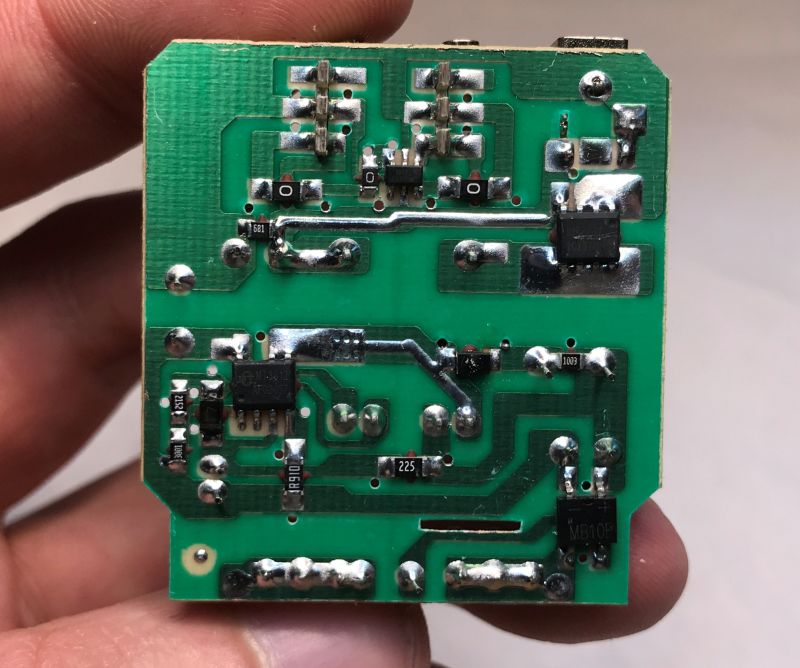
We only have a fuse at the input, and then there is a rectifier bridge. Then the minimum inverter circuit:
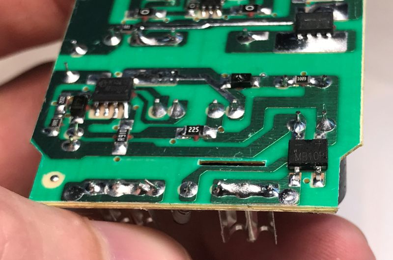
You can easily read that the inverter is based on the MT3612:
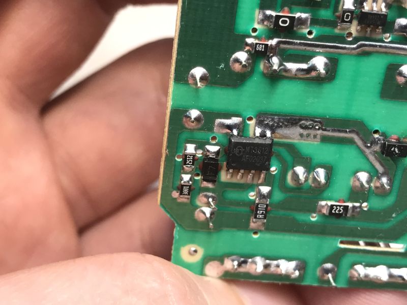
This fully dispels any doubts - according to the catalogue note, we have here up to 10/12 W depending on the version:
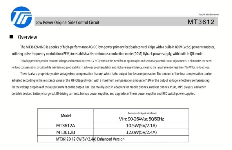
9bb358427
Now we look at the secondary, low-voltage side.
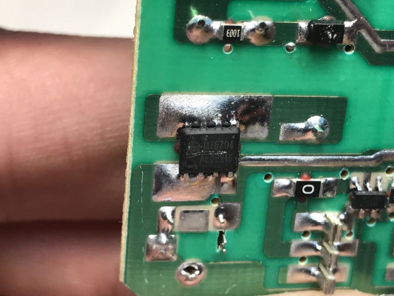
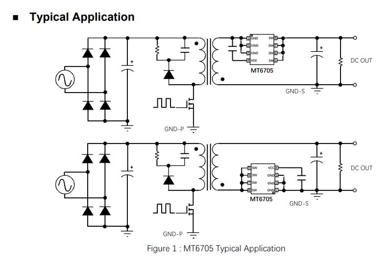
There is only one more modern aspect here, as we have an MT6704 synchronous rectifier (based on a MOSFET) instead of a Schotky diode:
Practical tests
To start with a current of 1.5 A:

After half an hour the main PSR controller approaches 50 °C, the synchronous rectifier heats up a little less.
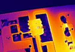
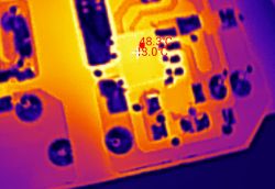
This is very strange, but after a momentary load of 1.5 A the voltage starts to jump to 6.5 V.
What happens, on the other hand, when we increase the current?


At this load, the systems exceed the 50 °C limit.
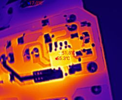
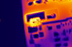
The voltage is also able to occasionally drop to 3.4 V, i.e. the overload protection is trying to protect the inverters.
Summary
This product is outright misleading and does not deliver what is promised. What's more, the whole thing is of poor quality, and after a load of about 3 A the voltage starts to jump in a strange way, up to 7 V, and the overcurrent protection does not always immediately engage.
In addition, the construction is flimsy, I would be afraid that at some time of pulling out of contact a part of the device will be left in my hands.
I wonder what the construction of the transformer is like, but I didn't want to destroy it to find out.
All in all, it is hardly surprising that I would totally advise against buying this product. If this is what a "welcome deal" or a "welcome gift" is supposed to look like, then I dread to think what the actual "cooperation" will look like. The shop is still promoting it and non-technical people are ordering and getting fooled.
Have you also come across this kind of electronic trap in online shops?


Comments
Something occurs to me that someone already showed a similar power supply/charger of 65W only in yellow that year. Interestingly, he also rated it as electro-junk. [Read more]
Most importantly, they didn't forget to give free 'plasticine'. [Read more]
Plasticine is added for two reasons. 1. To increase customer confidence in the product by increasing the weight of the product. 2. With loose web sockets, gravity improves contact. [Read more]
Nothing has changed for years, although the price should immediately "set off a red light". I used to do a lot of shopping on "Ali" and in many cases I was met with disappointment although I will honestly... [Read more]
What's the price, what's the product, after all, for US$1 you shouldn't expect miracles from majfriends. [Read more]
And so I'm surprised it works after all, for that £4 you can only expect a case. [Read more]
I am a living (fortunately) example of how, when pulling such a charger out of the socket, the casing can stay in your hand and the live pins stick out of the socket all the time. [Read more]
What surprises me most anyway is that it is called a "welcome gift" - a welcome gift? After all, rather such a gift should discourage further purchases on the site, unless seriously customers are that... [Read more]
If someone burns down their flat because of such inventions, there will be a problem/ unfortunately, the liberalism of the free market allows it - the devices are not checked and allowed for sale. As for... [Read more]
And see, you've done us in. It's not the price of this charger for everyone, it's actually a welcome gift to those making their first purchase. Such prices appear as you view Aliexpress as not logged in.... [Read more]
And it's clear you didn't read from the beginning "I invite you to test the lavishly advertised welcome gadget offered to us by AliExpress for just £4 with free shipping." [Read more]
Ali has no welcome goodies. Those who register for the first time for almost EVERYTHING have an "occasional" price and free shipping. The $1 price was referred to by the author a few times later in the... [Read more]
I know it's a scam, you know, the author of the post wrote as above, he didn't emphasise that it's a "gift" for those who open an account. [Read more]
I, recently, was looking for a charger above 65W to charge my laptop and phone/headphones at the same time. I found 3 chargers priced at 100£+ with a claimed power output of ~100W. After testing under... [Read more]
I've also been using one for one of my older Macbooks for over 3 years/done over 200, 120W-USB-C, previously I bought ala the Apple original for about 100 and it was lame, and a brand new original for... [Read more]
I wrote a year ago that it was a dump. https://www.elektroda.pl/rtvforum/viewtopic.php?t=4097473 [Read more]
I once bought a 120W charger from majfriends, such a beautiful yellow one, 4 USB ports including 2 USB-C with a silver border. Of course, it had the same power as the one in the topic - 10W. A piece of... [Read more]
In my opinion, the EU should introduce a law prohibiting the sale of goods with incorrect specifications (plus some penalties to discourage such practices). I am not in favour of banning the sale of crap,... [Read more]