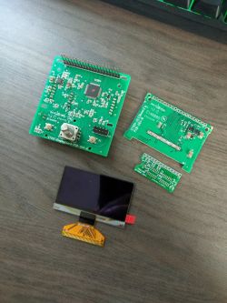
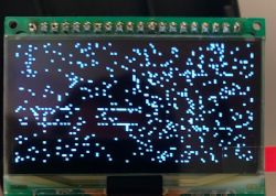
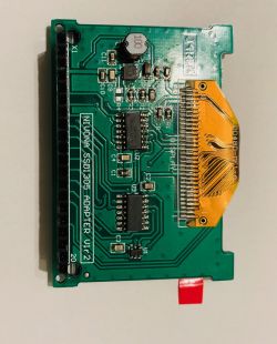
Unfortunately, the second attempt - I did not manage to start the module with the adapter - I dismantled and reassembled it very carefully - dead.
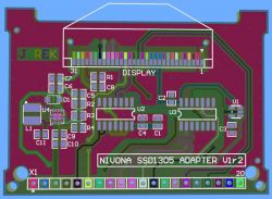
So I would like to assemble such a full control module for OLED according to the J4rek rev.2 project.
I would just like to clarify the issue of the elements - please check if I wrote it down correctly from the diagram:
NIVONA MODULE J4rek for 1305 display - version: full PCB, as in the attachment:
SMD BOM LIST:
L1 - 10uH SMD wire choke 10uH 0.4A 560mR 4.5x3.2mm H = 1.5mm
D1 - MBR0530 Shotki diode 30V 0.5A
C1 - 4u7 / 16V
C6 - 4u7 / 16V
C7 - 4u7 / 16V
C8 - 4u7 / 16V
C10 - 4u7 / 16V
C11 - 4u7 / 16V
C2 - 100nF / 16V
C3 - 100nF / 16V
C4 - 100nF / 16V
C9 - 100nF / 16V
C5 - 22pF
R1 - 1M
R2 - 1M
R3 - 120K
U1 - SN74AHC1G00DBVR
U2 - CD4071B
U3 - CD4078B
TPS61045 TPS61045DRBR QFN-8 Chipset IC REG BOOST ADJ 0.3A, LED driver, 1 output, boost (step up), 1.8V-6V input, 1MHz switching, 28V / 20mA output
--------------------------------
I just started my adventure with SMD .
1.
I have a very lame question about the size of the SMD components needed for this PCB -
elements should be 0603 or 0805 size ? The size 1206 capacitors I bought turned out to be a bit too big and not very convenient to solder in the fields.
I left the integrated circuits and OLED display from the experiment with a small adapter, I miss C5 - 22pF, R1 - 1M, R2 - 1M, R3 - 120K, I will sell the rest.
2.
The last question - does anyone have one or two bare laminates of the full PCB J4rek rev. 2 and can help me and resell at cost, possibly with these missing SMD C5, R1, R2, R3 components? Or maybe a damaged NIVONA display module with a working motherboard for little money, so that it does not lie in a drawer and help me revive my Nivona?
