 .
.
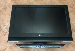
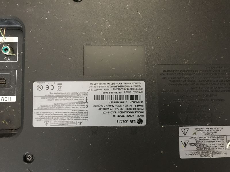
Today another short presentation of the inside of an old piece of equipment. This time it will be a 32-inch LG LCD TV premiered in 2007, equipment still with fluorescent backlighting, a screen with a resolution of 1366 x 768 pixels. I'll show its interior here and see if anything from inside can be useful for DIY construction.
 .
.
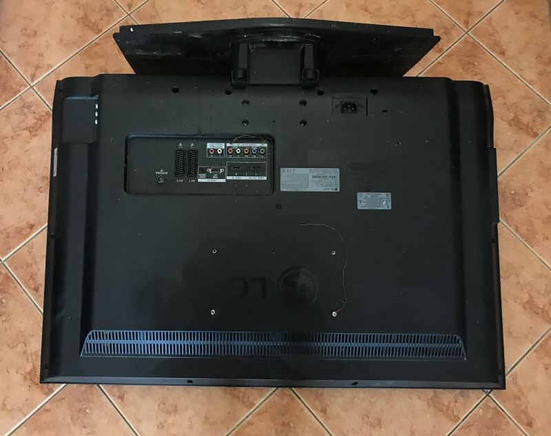
On the back we have mainly two HDMI ports, two SCART connectors, component and S-Video inputs and an RGB (PC) input. There is also already a rather useless antenna connector - because the TV does not support the DVB-T2 standard, so it will not receive the current digital terrestrial TV channels without an additional tuner.
 .
.
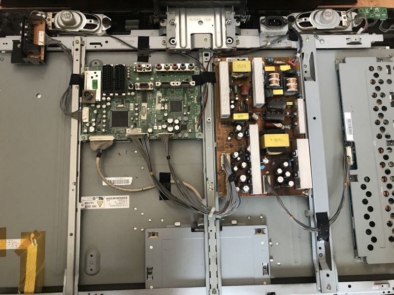
After removing the rear casing, it is immediately apparent that there are far fewer electronics inside than in plasma TVs. Here we have separately the power supply module, separately the main TV controller module (video processing), and separately the board with the inverter powering the fluorescent tubes. In addition, you can also see the speakers and some side two boards, one with the IR receiver from the remote control, the other with the video connectors.
 .
.
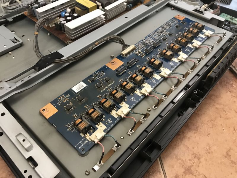
Here is the board with the fluorescent power supply after removing the metal shielding:
 .
.
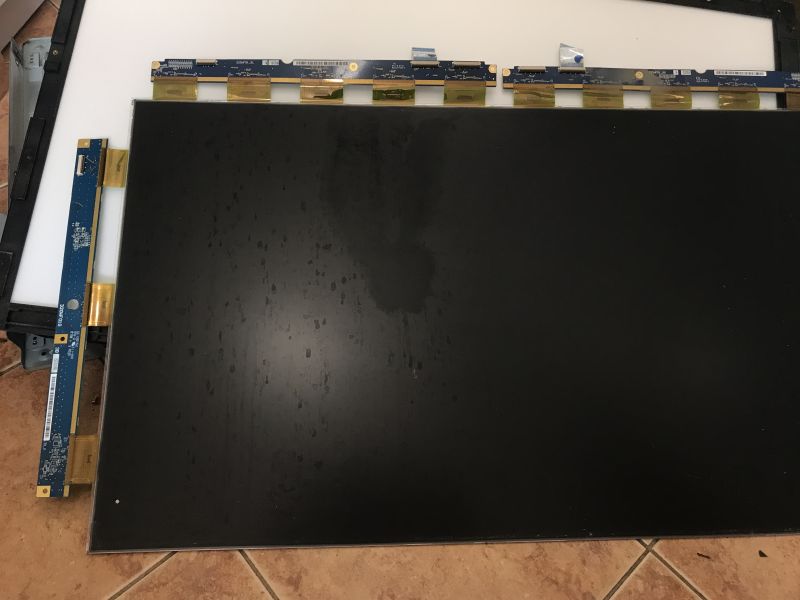
Further disassembly reveals an additional module - the T-Con - or Timing Controller. The T-Con deals with the control of the matrix, with the LVDS signal being applied to its input. The LVDS itself can be generated from a universal matrix control board, but the T-Con is unlikely to be replaced by a universal board. There have already been topics about LVDS:
Laptop LCD matrix as independent monitor .
The second life of a TV with a dead motherboard as a DIY VGA monitor - (anti)guide .
There are fluorescent tubes behind the matrix, but this is where I didn't look anymore:
 .
.
It's now time to look at the plates.
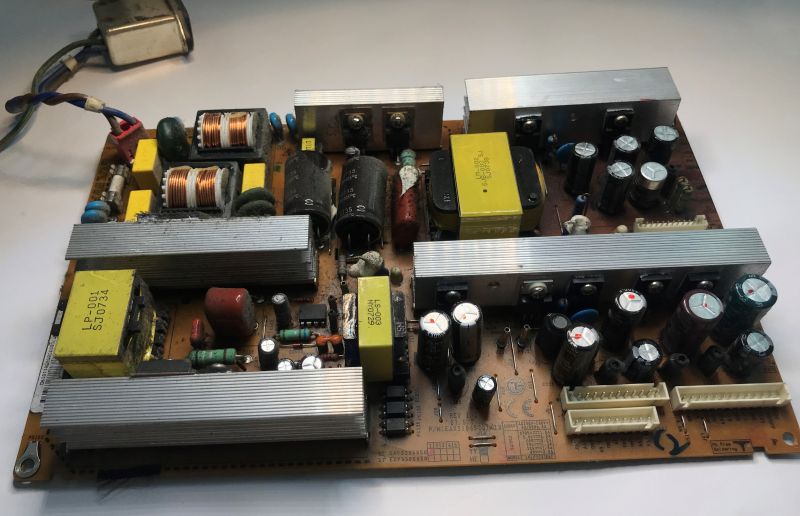
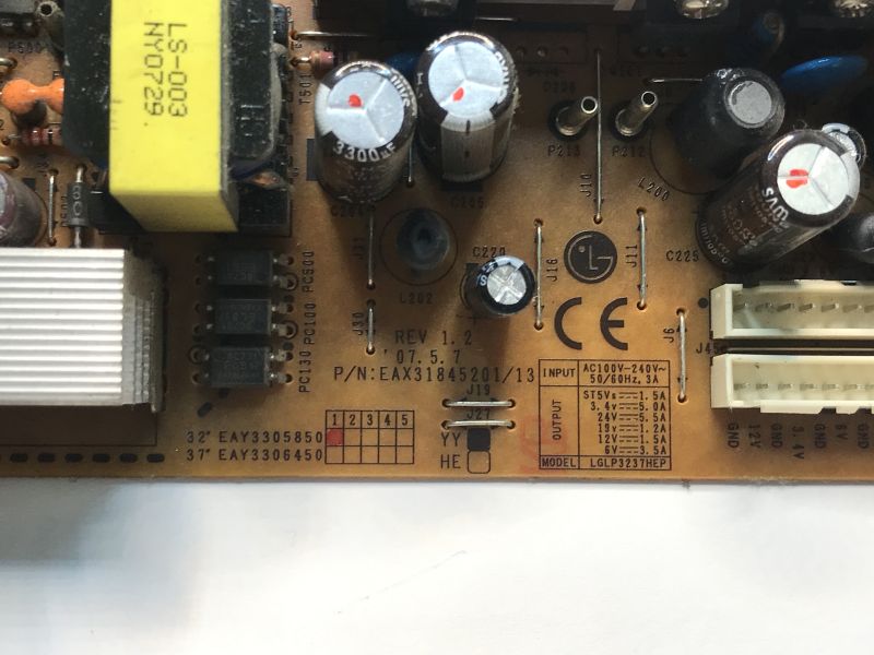
The power supply is REV 1.2 07.5.7 P/N: EAX31845201/13 - 32" version EAY33058501.
 .
.
The power supply module gets the mains voltage at the input and generates lower DC voltages for the rest of the TV. In this case these are 5V standby, 3.4V, 24V, 19V, 12V and 5V, as printed on the board.
 .
.
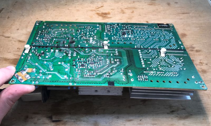
The board itself is primarily made in through-hole assembly, with only a few components surface mounted on the underside of the board. These include the inverter controllers.
 .
.
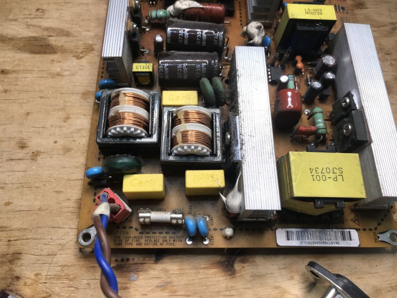
At the input of the board we have extensive filters and surge protection, a fuse is of course also present.
 .
.
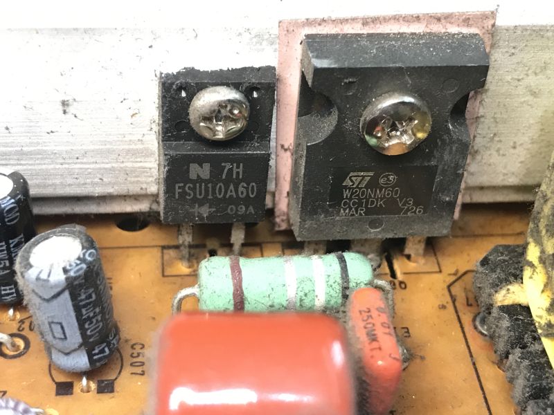
Next we have a circuit which I have described as an active PFC:
 .
.
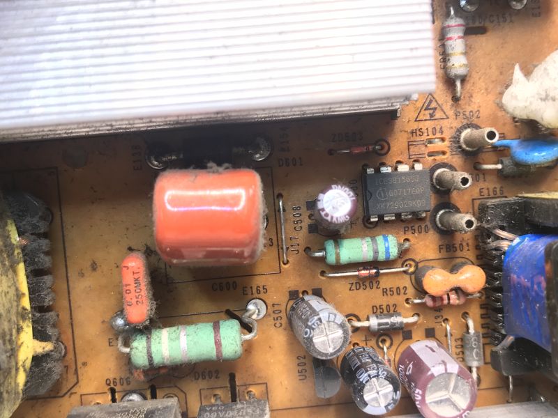
Standby is implemented based on the ICE381565J:
 .
.
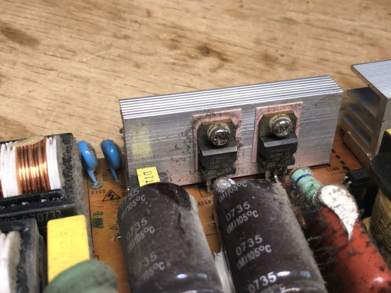
The main inverter appears to be a half-bridge, based on two identical P9NK60Z transistors:
 .
.
The power supply from the backlight is a completely separate module. The whole unit is made on a thick laminate to dissipate heat effectively. All components are on one side and the soldermask is removed from the "feet" so that there is better contact with the rest of the TV skeleton.

 .
.
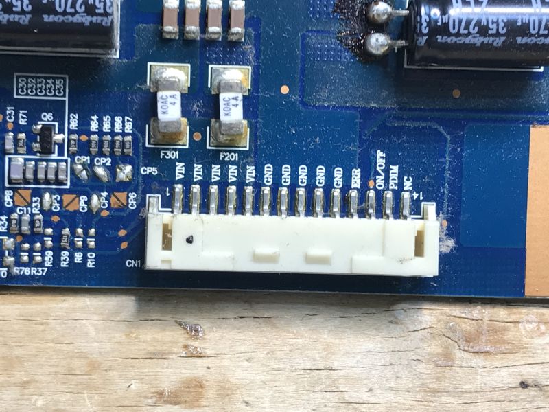
Getting this module up and running is very simple. Most of the wiring is ground and power, as there is a lot of current flowing. The supply voltage is probably 12 or 24V. In addition, we have the ON/OFF signal and PDIM (dimmer), the P probably stands for pulse/PWM, i.e. control by PWM. In addition, there is also an ERR signal (the controller reports an error with it) and an NC pin, which... is simply not connected.
 .
.
At the output, the circuit generates a high voltage for the fluorescent lamps - higher than the mains, generally around 1000V.
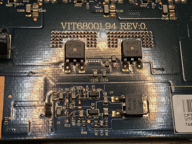
The greatest power is given off here by the transistors, of which there are as many as eight. They are soldered to copper spouts and vias facilitate cooling.
 .
.
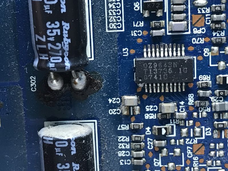
The main inverter controller from the backlight is an OZ964SN.
 .
.
 .
.
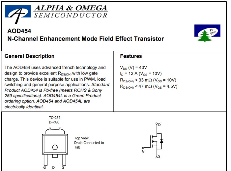
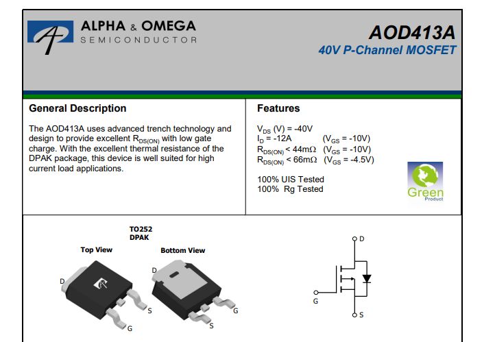
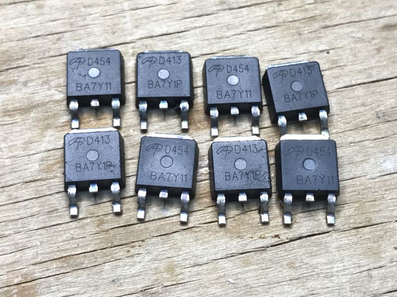
Rather, the most interesting transistors to recover here are D454 and D413. Complementary pairs.
 .
.
The low Vgs parameter shows that they can potentially be easily driven from the microcontroller.
They can be easily soldered out, but here hot air is already required.
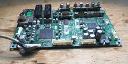
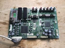
On the main board are the video signal inputs and also present is the RF tuner module. It is here that we essentially have a 'small computer', along with inverters to power the CPU and memory.
 .
.
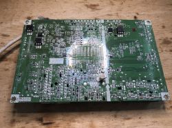
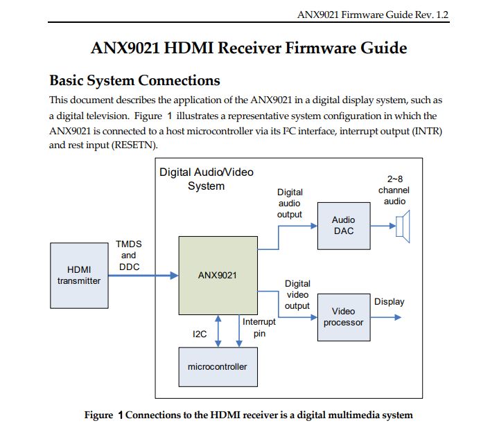
On the bottom of the board I can also see an EEPROM and some sort of LDO regulator. I'm more likely to recover Flash memory from this type of board, as in newer TVs you can get quite attractive sizes such as even a few megabytes, all while retaining the eight-legged case, but here I didn't see one. The rest of the chips are quite specialised and it's hard to make something out of that. Interestingly, on the other hand, the AXN9021 used here has fairly good documentation available on the web.
 .
.
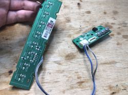
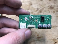
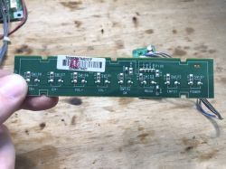
Of the finer things, that leaves the keypad and the infrared receiver, and here too you can note their design. The keypad has 8 buttons and only two signals go to them - KEY1 and KEY2. The buttons in turn have different resistors next to them.... and so presumably each button sets a different resistance, and the main controller reads the value analogue, via the ADC, and so determines what was pressed.
 .
.
That leaves the T-Con, here too the whole thing is one-sided:
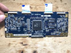
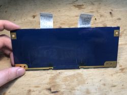 .
.
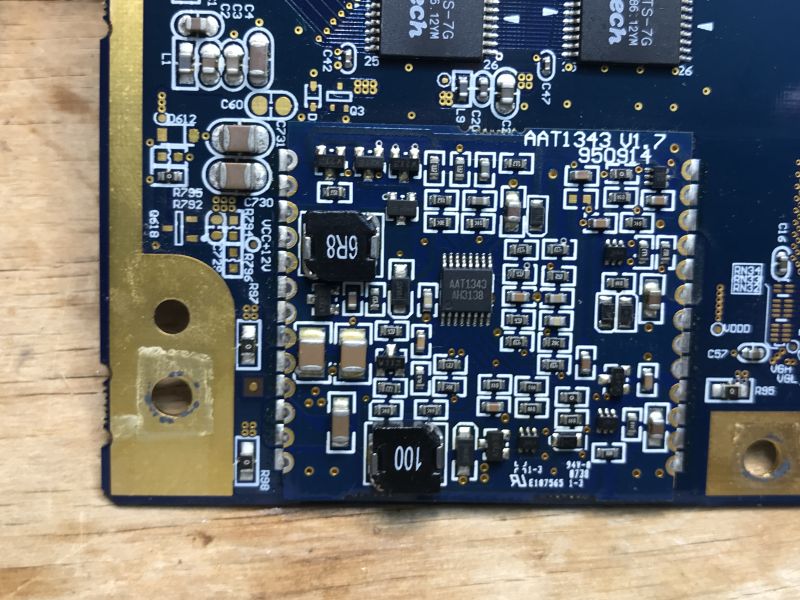
In its construction, I was surprised to find an additional, add-on AAT1343 V1.7 module. This is again an inverter - a PWM controller for DC-DC.
 .
.
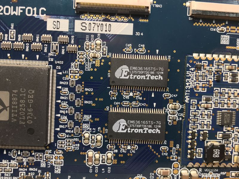
Also on the T-Con is a VTII8874 FL0258.1C processor and EM636165TS-7G (1M x 16 bit Synchronous DRAM) memories.
 .
.
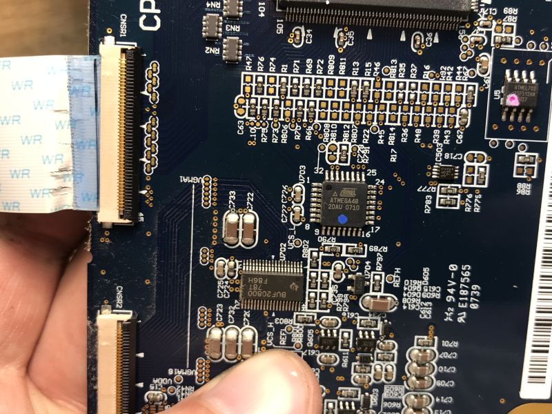
What caught my attention most, however, was the Atmega48 present here:
 .
.
I've done most PIC programming, although I've also played a lot with Arduino. I don't know the Atmeg itself directly, but it would probably be possible to hook up an ASP to it from USB and animate it for some DIY.
Summarising , inside we have a power supply generating low DC voltages from which the inverter for the fluorescent lights (generates a high voltage of about 1000V) and the main board processing audio/video signals are powered separately.
I find the very structure of the TV shown here quite rich, the division into boards, still these metal mounts, in newer copies there is not so much raw material. You can feel it even from the sheer weight of the receiver. I must soon show the interior of some modern, so-called "smart" TV with LED backlighting, these are already really light and also more difficult to disassemble.
In the context of DIY I managed to recover some parts, these transistors are attractive and easy to drive, and the Atmega is an unexpected bonus that I will run separately. Apart from that, you could play around with running the power supply, but it's not very practical, plus you could run the backlight inverter completely off the circuit, as its control is very simple, and do some DIY fluorescent lighting for the cabinet....
That's it for now, maybe it's of interest to someone. That Atmega inside is something I didn't expect myself....
PS: Now I see that the schematic of this power supply is with us on the forum, so if anyone wants to read it, just type it in the search engine... .
Cool? Ranking DIY Helpful post? Buy me a coffee.


