logo elektroda
logo elektroda
X
logo elektroda

Print positioning gadget for double-sided PCBs

efi222 1791 8
ADVERTISEMENT
Treść została przetłumaczona polish » english Zobacz oryginalną wersję tematu
📢 Listen (AI):
  • From my observations, fewer and fewer DIY builders are producing their own PCBs.
    This topic is dedicated to the handful of others who "agonise" over this subject:) Although they certainly have their own proven ways.
    I usually do one-sided plates for my needs and here I have mastered this 100%. However, the day came when I was forced to make a double-sided PCB.
    I tried various patents. With holes for positioning the sides, with envelopes and others, with various final results. I got tired of the centring holes. (Maybe I don't have the skill).
    In the end I came up with an alternative, experimental gadget that makes it easier to position the bottom and top print of the tracks.
    The mosaic to be printed has to be provided with a corner marker for both sides of the print, or a larger frame. According to this marker you need to cut one corner of the print paper for each side.

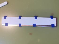
    I align the plate with the adjustable "pressers" to the corner of the jig. I place the printed paper on the plate and fix it with pieces of paper adhesive tape.
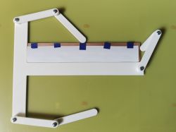
    PCB positioning jig with printed paper sheet taped to copper-clad board

    I cut the corner of the plate and the printed paper slightly so that there is a better fit between the sides and the frame.
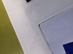
    Close-up of alignment jig corner with trimmed paper fitted into the frame

    I then turn the plate over and fix it in the jig.
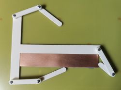
    PCB alignment jig with clamping arms and copper-coated board

    Continue analogously to the previous page.
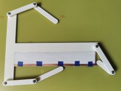
    PCB positioning jig with printed paper and tape on a green background
    PCB board with printed paper aligned and taped with blue painter's tape

    The arms are connected by sunken inserts with M3 threads.
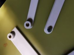
    Close-up of a white mounting jig with three arms screwed into a green surface.

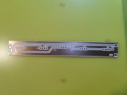
    Drilled inserts. 2.1mm diameter through-hole pads. Deviations are and probably always will be. This is the third tile I've done this way. It's not too big - 170x30 mm. I haven't tested on larger sizes. But the potential I think is there.
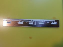
    Double-sided PCB with etched traces and alignment holes on yellow background
    Narrow double-sided PCB with white traces and mounting holes on a copper surface

    I need to observe in which phase these shifts occur. Maybe something can be refined further.
    And that's all. Greetings :)

    Cool? Ranking DIY
    About Author
    efi222
    Level 21  
    Offline 
    efi222 wrote 630 posts with rating 1041, helped 12 times. Live in city Toruń. Been with us since 2019 year.
  • ADVERTISEMENT
  • #2 21635363
    mmaker
    Level 19  
    Hi! Quite a cool idea, if it makes the work easier, it's a success, as I myself often make double-sided PCBs for my needs and sometimes feel that it would probably be better to order and wait than to do it myself at home. As for thermal transfer, I personally do it differently in double-sided boards. I print both sides of the PCB on chalkboard paper, with one print on just one side left longer and the other print on the same side cut shorter, so that there is the possibility of later gluing these prints together with a layer of toner to each other using kapton tape. I then separately dry the paper with the print on an iron until the toner starts to shine. After assembling and marking the holes under a light or on an old monitor matrix with the backlight on, I tape the two printouts together on one side. After this I have the paper ready for ironing. I cut out the PCB laminate along the contour, clean, dry and degrease it. Then on a piece of plywood prepared for thermal transfer I place a cotton cloth or other piece of cloth, on this I place a sandwich of the print and in the middle I put the laminate. Then I put another cloth on top and the PCB is ready for ironing. Unfortunately it sometimes happens that the holes after ironing diverge by about half a millimetre then I remove the toner from the board and the whole procedure flies again, or sometimes if the paper is inadequately dried then I get blisters which are then impossible to remove :D Such a fate unfortunately ;) I tried to print on special yellow paper but this has a tendency to crack the toner when bending, I also tried the photochemical method but I think in this case is even more work and there is also the problem of the double-sided PCB holes. I also tried varnishing the laminate and burning the paint with a 5W laser, but the first tests turned out to be average, so I will still try this method.
  • ADVERTISEMENT
  • #3 21635382
    efi222
    Level 21  
    Thanks for the response :)
    I did my first attempts with positioning holes too. The next with positioning the corner of the print with the corner of the plate. In the second case it is easier to achieve good results (in my opinion). This jig makes it easier to align the corners. I use a laminator for ironing, so it's a slightly different technology compared to an iron.
  • #4 21635513
    gregor124
    Level 27  
    I at one time developed my own method for making PCBs.
    I modified an old HP laser printer by pulling its fuser outwards so that when printing, the paper bypassed it, so that the applied toner was not fixed.
    The toner adhered well to the paper (I sometimes used laser printer film), so that the drawing could be accurately applied to the laminate without any problem.
    Then, with the help of a brush on the other side of the paper, I gently tapped the drawing (toner) onto the laminate.
    Finally, I heated the laminate to fix the toner.
    If necessary, the operation could be repeated. The paper or film could be used several times.
    Helpful post? Buy me a coffee.
  • #5 21635531
    Krzyychu
    Level 14  
    I made my last double-sided board a very long time ago, but somehow it didn't cause me any problems. First I printed the tracks on a laser printer and chalkboard paper and folded them under the light to make the vias meet. I taped the three sides together to make an envelope, inserted the board inside, fixed it with tape so it wouldn't move inside and put it in the laminator. Some movement did occur, but it was minimal.
  • ADVERTISEMENT
  • #6 21635643
    acctr
    Level 39  
    As I was recently making a double-sided PCB by my own efforts in the editor I copied the Top layer, reflected relative to the longer edge and moved it by the thickness of the laminate (1.6 mm I think). I got two drawings this way, where I only included Bottom in the base one. I bent the print at the edges and everything fitted together perfectly.
    The paper needs to be thicker to avoid jitter and it's best to bend the free edges at the start.
    Obviously a PCB design oriented to minimise connections between layers, especially under the DIP elements.
    Helpful post? Buy me a coffee.
  • ADVERTISEMENT
  • #7 21635664
    efi222
    Level 21  
    I know from experience that it is also a good idea to run a blank sheet of paper through the printer, for heating before printing proper. The paper I have shrinks about 1mm when heated on the printer. The phenomenon is already very limited by the second printing.
  • #8 21636187
    LA72
    Level 41  
    efi222 wrote:
    Corner of plate and paper with print slightly cut so that there is a better fit between the sides and the frame.
    Close-up of alignment jig corner with trimmed paper fitted into the frame


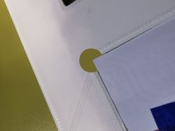
    As you are designing for corners you can make rounds.

    White rounded corner with flat material installed on green background

    You will be able to use tiles without chamfers.
  • #9 21636205
    efi222
    Level 21  
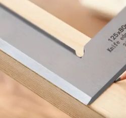
    Good point. The scribe angles have a similar dodge.
    Close-up of a try square positioned on the corner of a wooden board
    I also thought of this as the hardware was already in use :) So much so that even with the hole in the corner there will still be a slight protrusion at the start of this rounding. Alternatively, it can be refined.
📢 Listen (AI):
ADVERTISEMENT