In a static regime, MOSFETs provide maximum performance and their power efficiency is quite high. When dynamically driven, however, their efficiency can be compromised and power losses inevitably increase. LTspice, and in general any software implementation of SPICE, does not have functionalities to manage the thermal behaviors of an electrical circuit or a specific component. But with some thermal model implementations, it is possible to predict a number of temperature simulations. In this tutorial, we will see how to set the ambient temperature of a SiC MOSFET and visualize its behaviors.
Thermal SPICE models
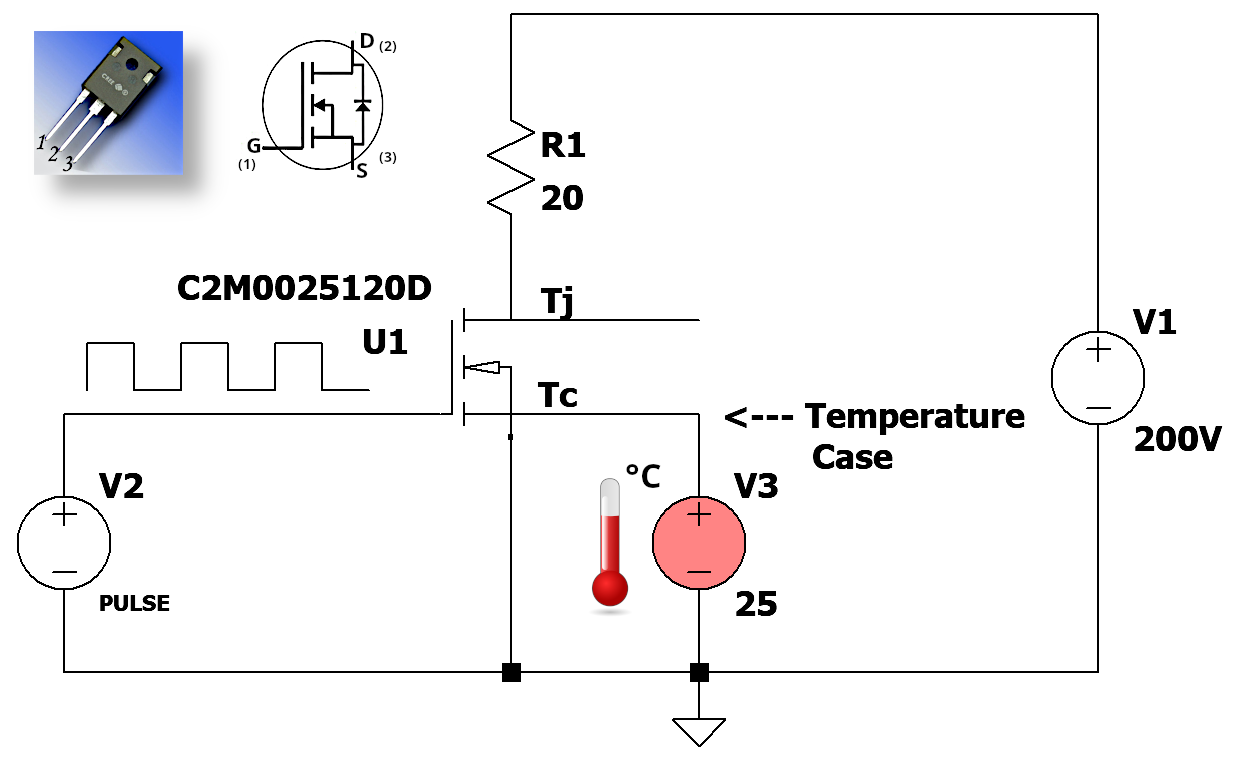
There are new SPICE models, especially with regard to MOSFETs and power diodes, which manage to implement, roughly, the thermal behavior of an electronic component. In a simulated circuit diagram, it is easy to recognize them because they are equipped with two additional terminals tasked with handling temperature-related parameters. Specifically, Tj and Tc terminals are included in the model to analyze the heating of the device as a function of time. Terminal Tc represents the temperature of the case and Tj the junction temperature.
The temperature connections work exactly like the electrical voltage pins, except this quantity identifies the temperature and they are electrically separated from the circuit. Therefore, a voltage of 1 V across these terminals refers to a temperature of 1˚C. The two terminals, Tj and Tc, can be used both to read working temperatures and to set them to desired values. In the following examples, we will study precisely the second aspect. So the voltage at node Tj contains information about the junction temperature as a function of time, which in turn operates directly on the electrical model as a function of temperature. The terminal Tc must be connected to a voltage source (which indicates the temperature of the case) or to an external RC network (heatsink model) to observe its effect on the junction.
Performance analysis of a SiC MOSFET at various switching frequencies
The practical example shown below (see circuit diagram in Figure 1) uses a SiC MOSFET model C2M0025120D with the following characteristics:
• Vds(max): 1,200 V
• Id: 63 A
• Id(pulsed): 250 A
• RDS(on): 60 mΩ
• Package: TO-247-3
• Vgs: between –10 V and 25 V
• Pd: 378 W
• Tj: between –55˚C and 150˚C
The scheme shows a SiC MOSFET driving a 20-Ω resistive load with a 200-V supply. When the MOSFET is closed, a current of about 9.98 A flows through the load. In the scheme, the MOSFET is driven by a voltage of 25 V. Depending on the operation, this voltage can be fixed for static operation or pulse-width–modulated (PWM) for dynamic operation. Depending on the case, the efficiency of the MOSFET is different.
The SPICE model of the MOSFET used in the wiring diagram is peculiar in that, as mentioned earlier, it has two additional terminals that are used to manage temperature. Connecting a voltage of 25 V to its Tc terminal effectively sets the temperature of its case at 25˚C. Therefore, this value does not refer to an electrical voltage but to a temperature. With this in mind, it is now possible to verify the dissipation of the MOSFET at a given temperature and under the different conditions of static and dynamic regime.
 Figure 1: The wiring diagram for the analysis
Static regime
The static regime involves driving the gate terminal with a fixed voltage (the maximum recommended by the component datasheet). In the conduction condition, the MOSFET works at its maximum efficiency, provided that the gate is driven with the correct voltage. There are, likewise, no power losses (except for the first few microseconds of conduction), as the voltage across the gate is fixed and continuous. In the diagram above, the fixed gate voltage is 25 V, and it causes the net conduction of the device. Running the simulation returns the following operating conditions:
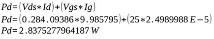
• Current on resistive load R1: 9.98 A
• Voltage Vds: 284 mV
• Power dissipated by the MOSFET: 2.8369 W
• Power dissipated by the load: 1994.3 W
• Efficiency of the circuit: 99.857953%
As can be seen from the results in static regime, the efficiency of the system is very high due in part to the low value of the RDS(on) parameter of the MOSFET. Please note that to calculate dissipated power, the following relation can be used:
Gate current is quite small and, therefore, negligible.
Dynamic regime
In the dynamic regime, with a PWM signal characterized by a duty cycle of 50% and a voltage of 25 V, the average power dissipated by the device is half that of DC operation, as there is a conduction half-period and an interdiction half-period. The percentage of efficiency, in this case, changes in relation to the switching frequency and junction temperature. To carry out the analysis of the power dissipated by the MOSFET and the efficiency of the system, in the transient, the following SPICE guidelines should be used:

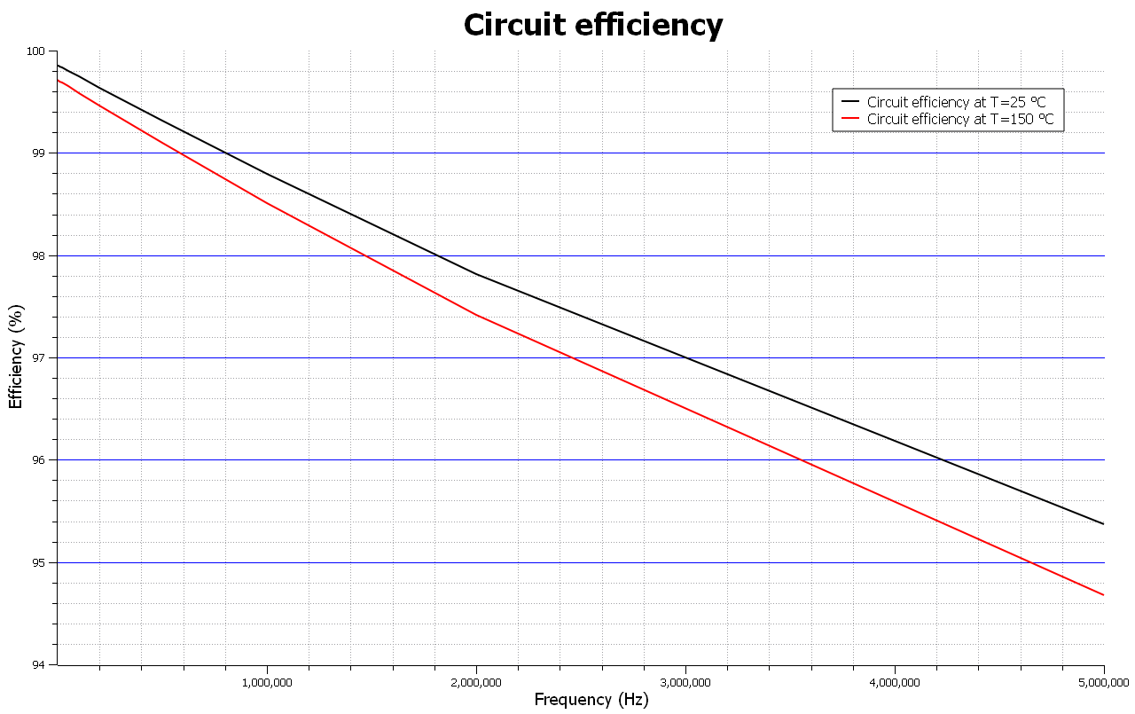
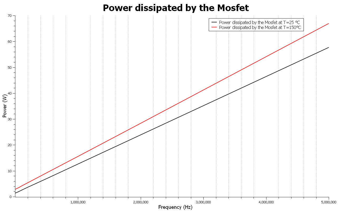
These simulation analyses allow us to observe graphs of the efficiency of the circuit in relation to frequency (see Figure 2) and of the power dissipated by the MOSFET, again at various drive frequencies (see Figure 3). As can be seen in the two graphs, the ability to change the temperature of the MOSFET case or junction allows for more accurate and realistic electronic simulations. The graphs refer to the same supply voltages of the circuit, the gate of the MOSFET and to the same value of the resistive load used.
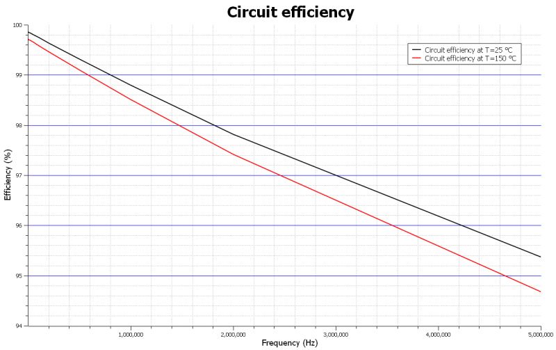 Figure 2: The graph of the circuit efficiency vs. the driving frequency of the MOSFET
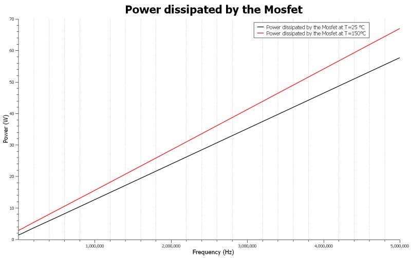 Figure 3: The graph of the power dissipated by the MOSFET vs. the frequency of its driving
In static regime, MOSFETs work very well due to their high input impedance and ability to drive very large currents. However, when they are to be driven by PWM, their efficiency may decrease. PWM involves a high switching frequency, which can cause high levels of thermal dissipation and reduce the life of the MOSFET. In addition, non-ideal response capabilities to rapid voltage changes can cause distortion and decreases in efficiency due to power losses. For these very reasons, it is always essential to use a good driver.


Comments