I would like to share an interesting observation after PCB assembly.
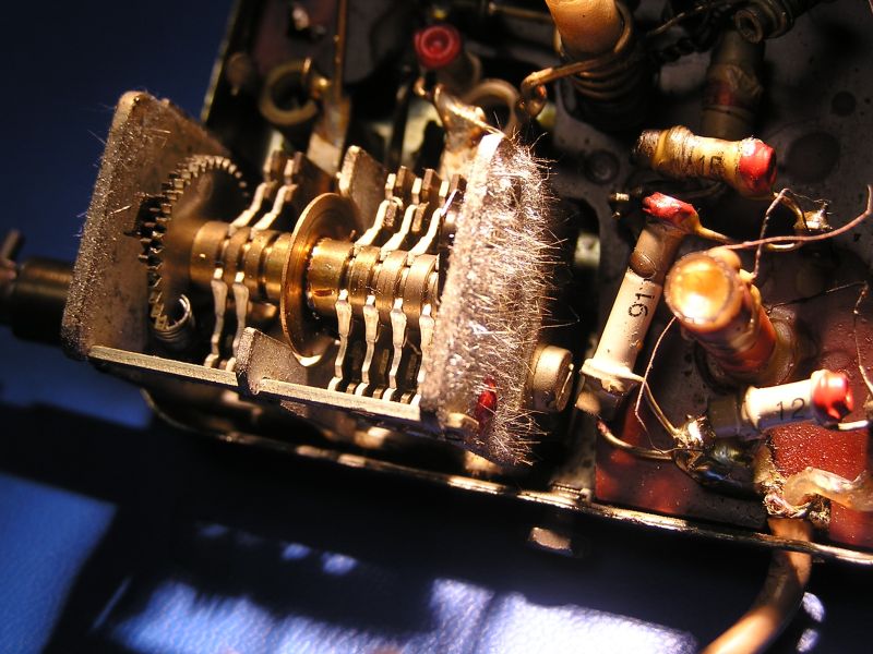
I was testing a device today whose PCB assembly of components I had commissioned 8 months ago. Lead assembly. The device failed the test due to unusual malfunctions. My initial thought was a faulty PCB, probably a micro short circuit. One or more. A former PCB supplier had incidentally made this type of error, despite a commissioned electrical test. I tried to find shorted tracks starting with the input circuits. To no avail. I started looking at the board under a microscope and eventually found the cause to be tin whiskers. The whiskers had grown on the input leads of the semiconductor actuators. You can read more about the subject of tin whiskers in Monika Jaworowska's article What is the danger of tin whiskers and how to avoid them?
The problem involved two ICs in housings with 0.5mm raster. The distance between the leads is therefore 0.2mm by catalogue. I am posting the pictures. Forgive the quality, but I only have a standard stereo optical microscope and had to take the photo through an eyepiece.

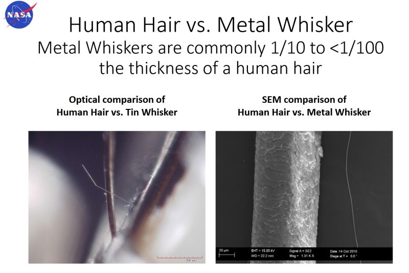
On the first element you can see a whisker that was already making a short circuit and another growing. The second element also had a whisker causing a short circuit. I estimate the width of the whisker (based on the photo) to be around 30-40µm.
After re-soldering the leads, the problem disappeared and the device works properly. Interestingly, on the first component, where 1.5 whiskers can be seen, they grew on the top of the leads, the whisker on the second component grew close to the PCB.
This is the first time I have encountered this type of fault in my devices. I recalled seeing a piece of clean tin. It contained a lot of strange hair-like structures on the outside.
I should point out in advance that I am approaching the subject from the practical side. What puzzles me is the cause of this type of structure and how to deal with it. My guess:
1. Excess solder paste applied to the PCB.
2. The paste was not mixed well enough before being applied to the PCB (?).
3. Residue of unleaded paste in the wrong ratio was left on the paste printer. Remnants of assembly of other boards (?).
4. Mechanical stress (?).
Points 2-4 I cannot verify, so they remain in the realm of conjecture. On the other hand, point 1 is insufficient for the problems described above.
I would like to flag up the problem and encourage Colleagues to discuss.
I was testing a device today whose PCB assembly of components I had commissioned 8 months ago. Lead assembly. The device failed the test due to unusual malfunctions. My initial thought was a faulty PCB, probably a micro short circuit. One or more. A former PCB supplier had incidentally made this type of error, despite a commissioned electrical test. I tried to find shorted tracks starting with the input circuits. To no avail. I started looking at the board under a microscope and eventually found the cause to be tin whiskers. The whiskers had grown on the input leads of the semiconductor actuators. You can read more about the subject of tin whiskers in Monika Jaworowska's article What is the danger of tin whiskers and how to avoid them?
The problem involved two ICs in housings with 0.5mm raster. The distance between the leads is therefore 0.2mm by catalogue. I am posting the pictures. Forgive the quality, but I only have a standard stereo optical microscope and had to take the photo through an eyepiece.

On the first element you can see a whisker that was already making a short circuit and another growing. The second element also had a whisker causing a short circuit. I estimate the width of the whisker (based on the photo) to be around 30-40µm.
After re-soldering the leads, the problem disappeared and the device works properly. Interestingly, on the first component, where 1.5 whiskers can be seen, they grew on the top of the leads, the whisker on the second component grew close to the PCB.
This is the first time I have encountered this type of fault in my devices. I recalled seeing a piece of clean tin. It contained a lot of strange hair-like structures on the outside.
I should point out in advance that I am approaching the subject from the practical side. What puzzles me is the cause of this type of structure and how to deal with it. My guess:
1. Excess solder paste applied to the PCB.
2. The paste was not mixed well enough before being applied to the PCB (?).
3. Residue of unleaded paste in the wrong ratio was left on the paste printer. Remnants of assembly of other boards (?).
4. Mechanical stress (?).
Points 2-4 I cannot verify, so they remain in the realm of conjecture. On the other hand, point 1 is insufficient for the problems described above.
I would like to flag up the problem and encourage Colleagues to discuss.
Cool? Ranking DIY


