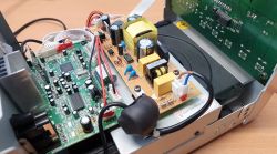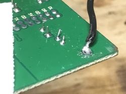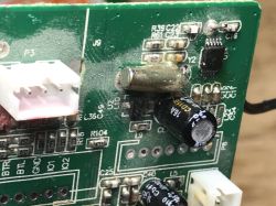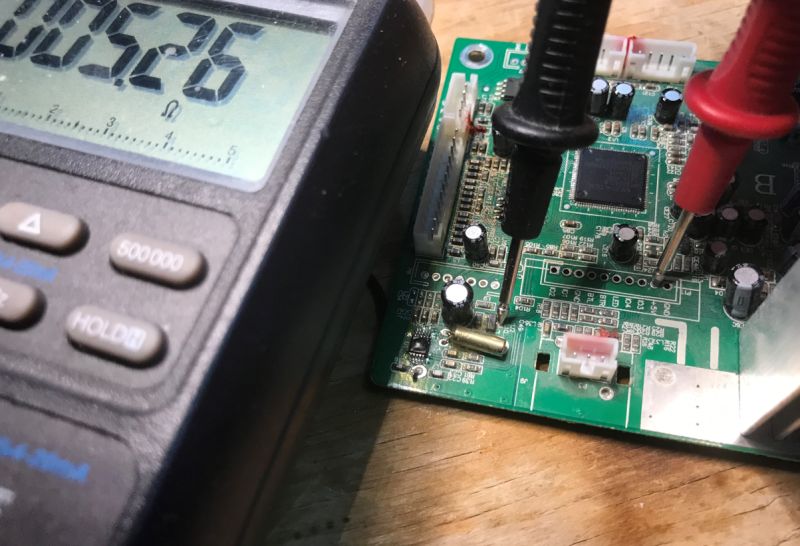
Here is a short presentation of the inside of the Blaupunkt model MS8BK microwave with CD and USB player. I will check here how it is built, try to analyse its firmware from an unknown microprocessor and determine its architecture in Ghidra, and then run its display with Arduino.
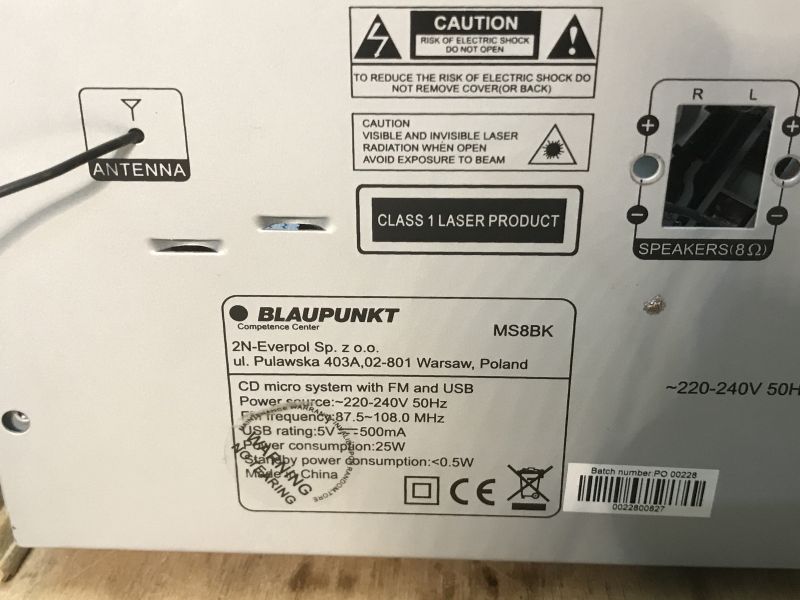
Interior of the MS8BK
The equipment came to me decomposed, so the presentation does not include the power supply. I can infer from the board itself that it provided standard voltages such as 5 and 12 volts. It was probably already a switching power supply in a flyback topology - the type I see in modern equipment. Older audio towers used to have the classic 50/60 Hz transformers, but I see them less and less nowadays.
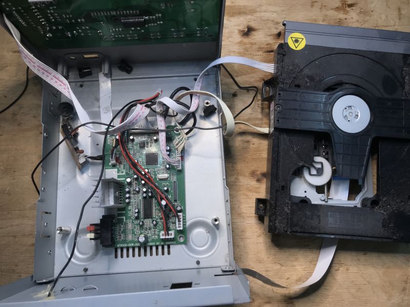
The motherboard rests on a Mediatek processor, I'll leave it for last. Right next to it you can see the 2 MB Flash memory, which perhaps houses the software, and in the corner there is also an EEPROM - maybe for configuration.
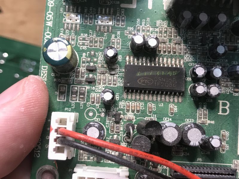
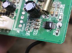
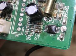
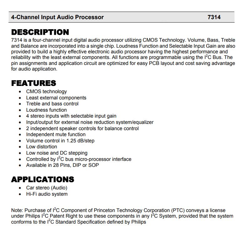
There is a separate four-channel processor for audio on the board - the PT7314E, the main CPU controls it via I2C:
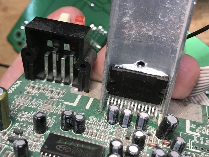
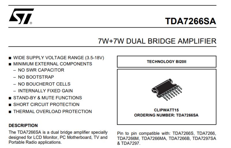
Separately, we have the amplifier - a dual 7W+7W, TDA7266SA, mounted on a large heatsink for adequate cooling:
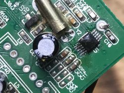
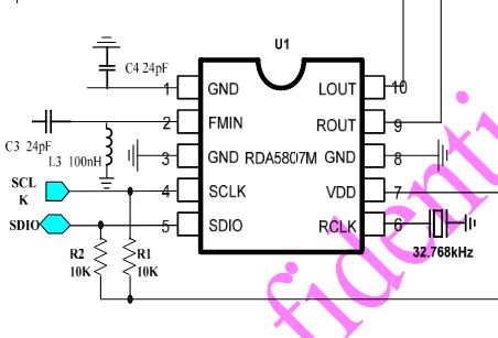
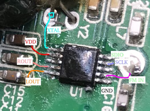
A watch quartz resonator and a small circuit in the corner still caught my eye - at first I thought it was an RTCC, but there's an antenna leading there. It's probably the radio's receiving circuit. Perhaps it would be possible to run it in bulk?
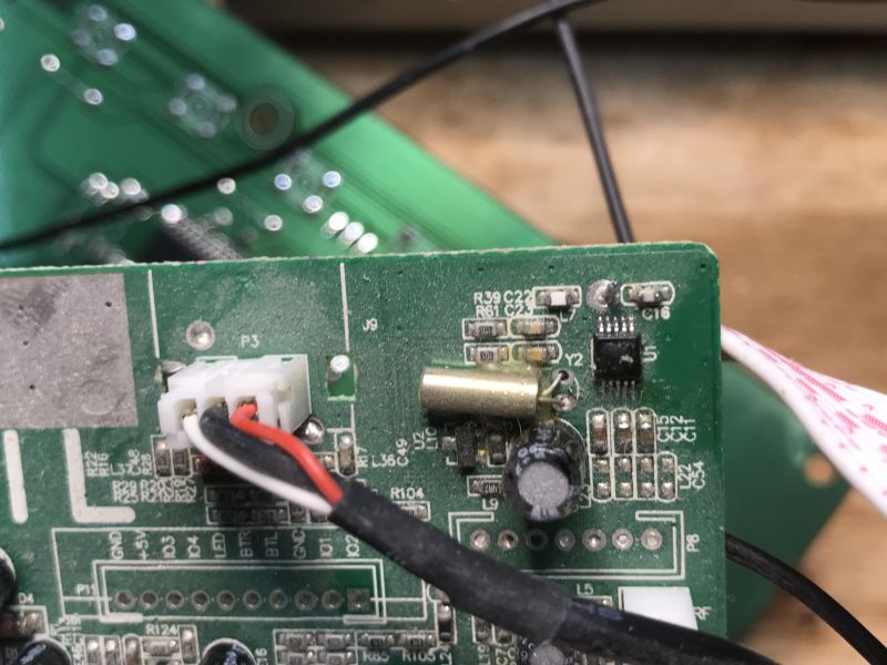
Well, that leaves the main MCU:
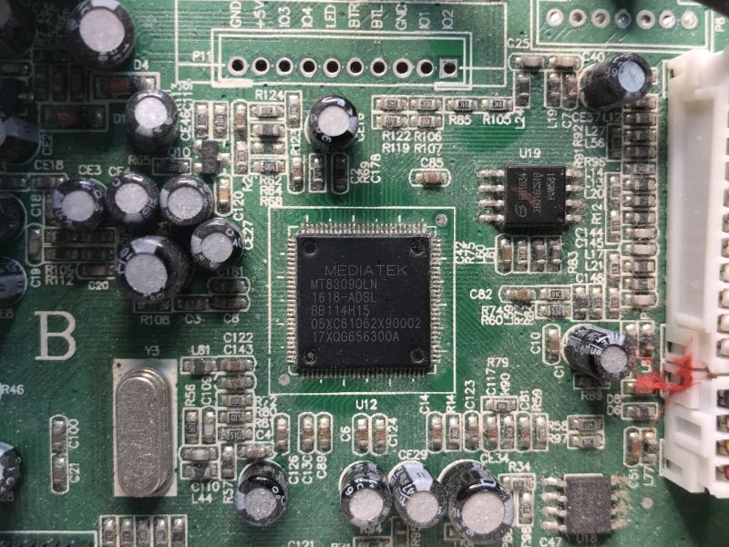
Mediatek MT8309QLN. I haven't found specific information about it on the web, although someone has already posted a batch from it on another forum:
Spoiler:
So the MS12BT has a very similar design.
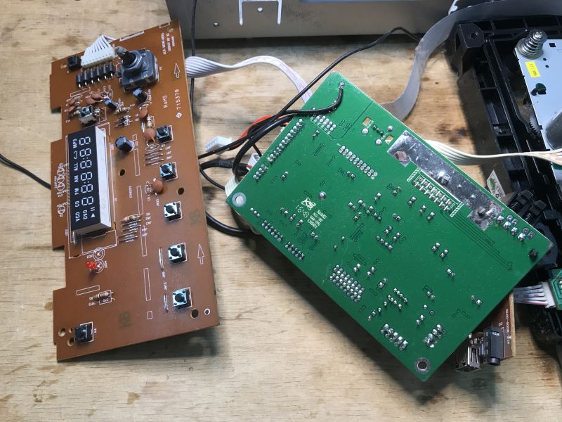
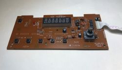
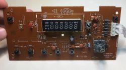
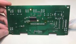
The display board is much simpler. The laminate is single sided, with only the main controller, the CD1628, surface soldered on the track side. It operates the buttons and the 7-segment display. In addition, we have an IR receiver, an encoder and a standby diode on the board.
Flash memory analysis
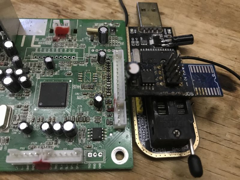
I soldered the Flash memory using hot air and read it with the CH341 programmer.
Binwalk found nothing interesting in it. I started looking through it in xvi32 . No header or partition structure is visible. The memory starts at bytes 02 1F E0, which is reminiscent of the 8051 jump instruction:
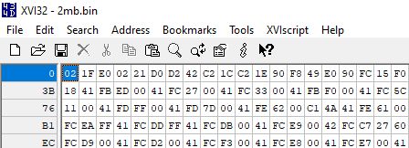
0x02 is the instruction code, 0x1FE0 is the jump address.
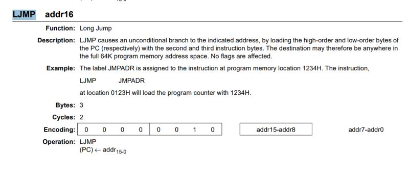
At offset 03 we again have jump instruction 02 21 D0. This matches with the interrupt position of the 8051. It looks like we do indeed have this classic core used here.
We'll try to decompile it, but it's still worth looking for ASCII captions, they can reveal a lot about the firmware.
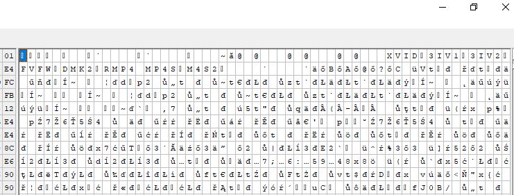
XVID, 3IV1, MP4S, M4S2 codecs.
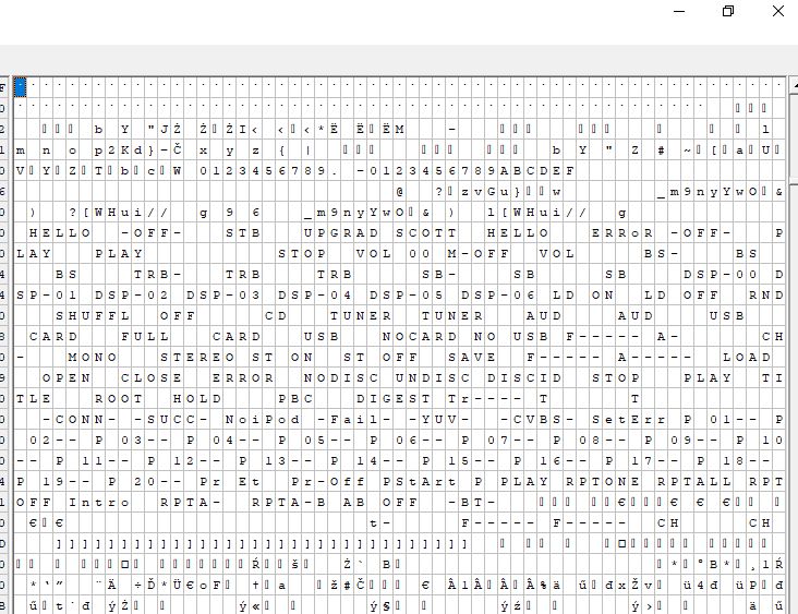
There's nothing more about booting or command line, so we probably won't run UART. UPGRAD only suggests batch updates. I wonder where SCOTT came from there - is that the author's signature?

MT1369? The internal name of the chip? There seems to be something wrong? Although here and here Mediatek....
https://www.elektroda.pl/rtvforum/find.php?q=MT1369
Looks like the chip from the DVD, strange. Maybe internally it's the same processor.
Time to move on though. I loaded the flash into the Ghidr decompiler and decoded it as 8051 instructions. The operations look correct, first we have a jump to the actual program from address 0x0, because we have interrupt vectors at the beginning:
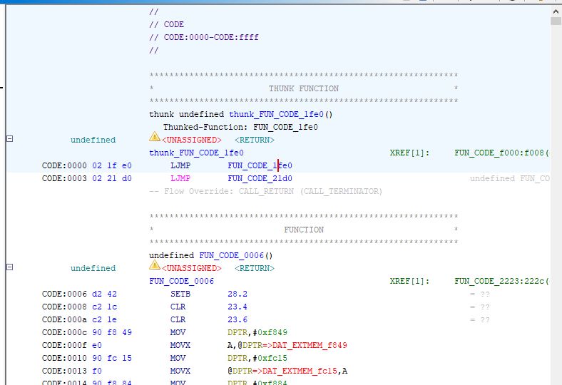
The first function resembles the initialisation of the three pins and the memory:
Code: C / C++
I also managed to find a separate function to initialise the timer, this clearly shows that the instructions are decoded correctly:
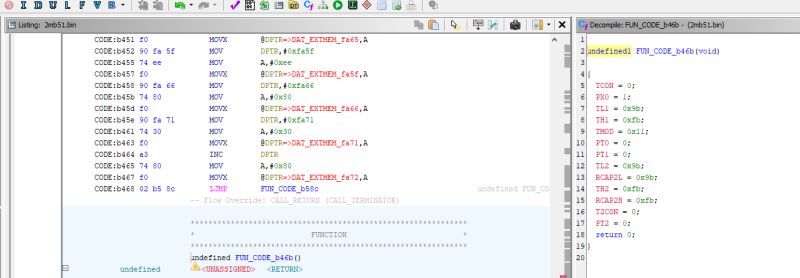
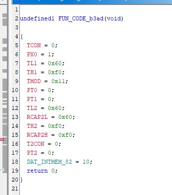
I've also looked for UART related commands, but haven't found anything that directly resembles sending or receiving, even though the standard UART registers of the 8051 are well documented and known.
Compare with the batch from MT1369?
However, I was curious as to why, according to our forum, the same writing appears in the memory dumps from the DVD.
I downloaded a copy of the batch from this post:
https://www.elektroda.pl/rtvforum/topic467658.html#2627620
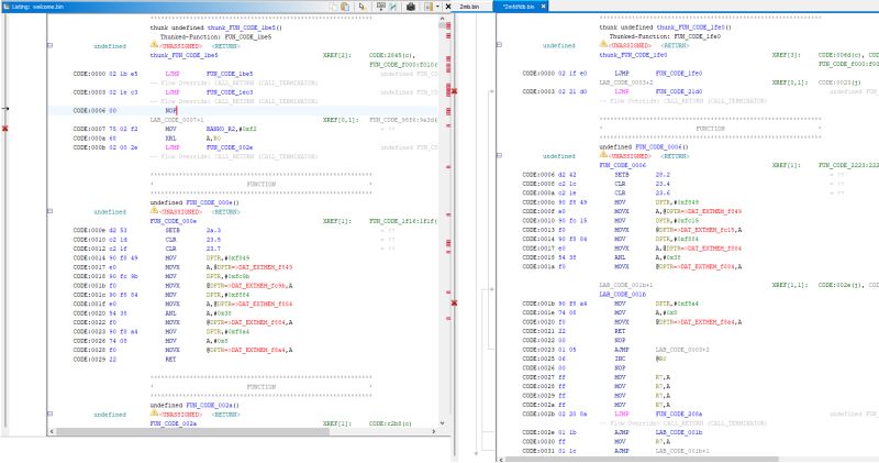
It seems to be the same initialisation process (or bootloader). A quick comparison of the two firmwares in Ghidra shows a very strong similarity.
Code: C / C++
This confirms the strong connection between the two firmware and the chips, although I did not perform a deeper analysis anymore.
I still made an attempt to compile a simple blink in SDCC for the 8051 but failed to detect any blink on the ports of my unknown processor. However, I don't know if it worked before - the radio supposedly had power and didn't start, so maybe there was something wrong with it before.
First step with the display
The display module is very attractive and useful - it doesn't require many pins to control, and it fits the watch just right. There are lots of digits, there are two colons, it will be worth the struggle.
You need to start with the CD1628 datasheet note. Fortunately, it is available:
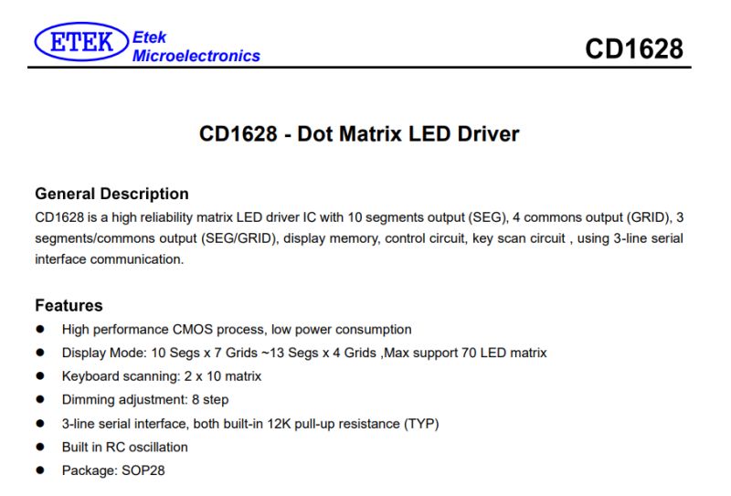
The CD1628 is controlled by three pins - DIO (data I/O), CLK (clock) and STB (strobe, chip select).
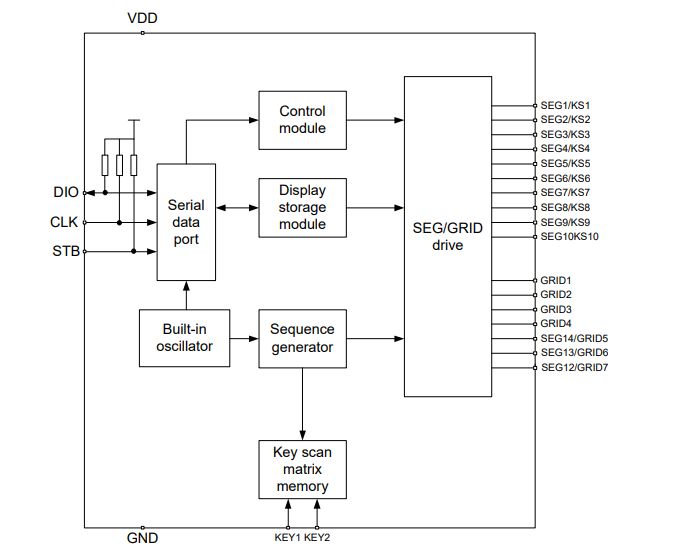
The protocol is described in the PDF:
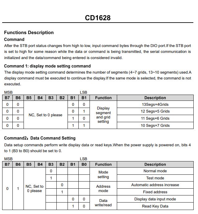
A quick read of the note tells us that this is essentially the same circuit as the well-known TM1628 family, TM1637, TM1650, etc:
We are running the HD2015 display/button controller after reverse engineering, comparison with TM1637itd
7-segment displays on TM1637 - 4 and 6 digits - Arduino, protocol
The main difference is that instead of generating I2C-style start and stop conditions here, we operate the STB pin here.
It's time to put this into code - I've chosen Arduino for simplicity:
First pins - 0 and 1 are RX/TX, so I started with 2:
Code: C / C++
Then sending data - according to the datasheet note.
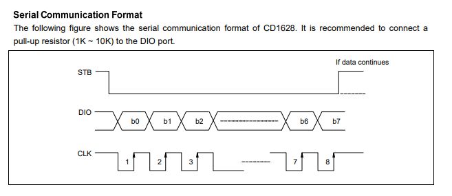
The bits are loaded on the rising edge of the clock, so I first set the clock to the LOW state, then set the DIO state, then wait a moment and reset the clock to the high state.
Code: C / C++
The strobe needs to be in the low state for communication, so I added an auxiliary function to send the command:
Code: C / C++
This is the basic build of sending.
Now the question is what to send.
The register addresses and commands are the same as in the TM1650 and similar .
Sequentially:
- Command 1 - setting the display mode (how many segments, how many grids)
- Command 2 - setting the operating mode (normal mode)
- Command 3 - setting display address and data (segments)
- Command 4 - setting the display control (brightness level, on/off status)
Code: C / C++
Here the only unknown is the first command - because we have four modes, how do you know which one is used on the board? Is it necessary to trace the paths?

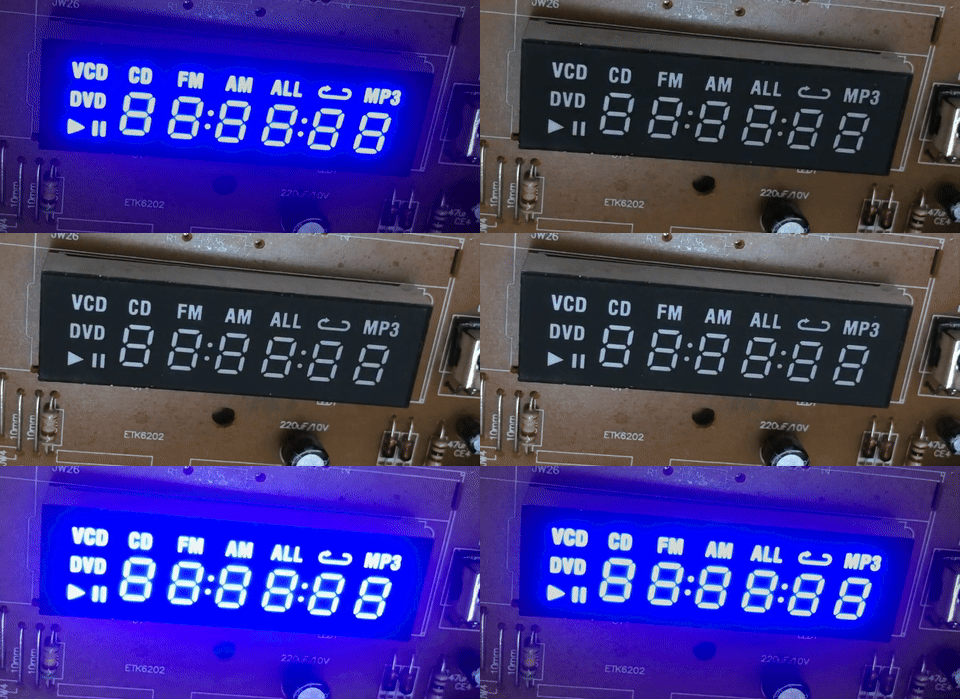
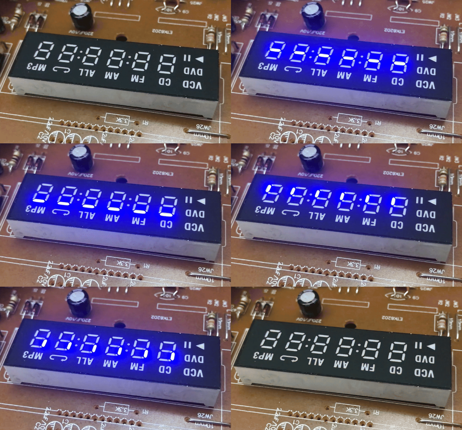
In my opinion, not necessarily - I just checked each of the 4 options and settled on the one that, with my test code setting all data alternately to 1 and 0, lights and extinguishes all fragments.
Code: C / C++
Result - first without setting the correct grid/segment configuration (0x03):
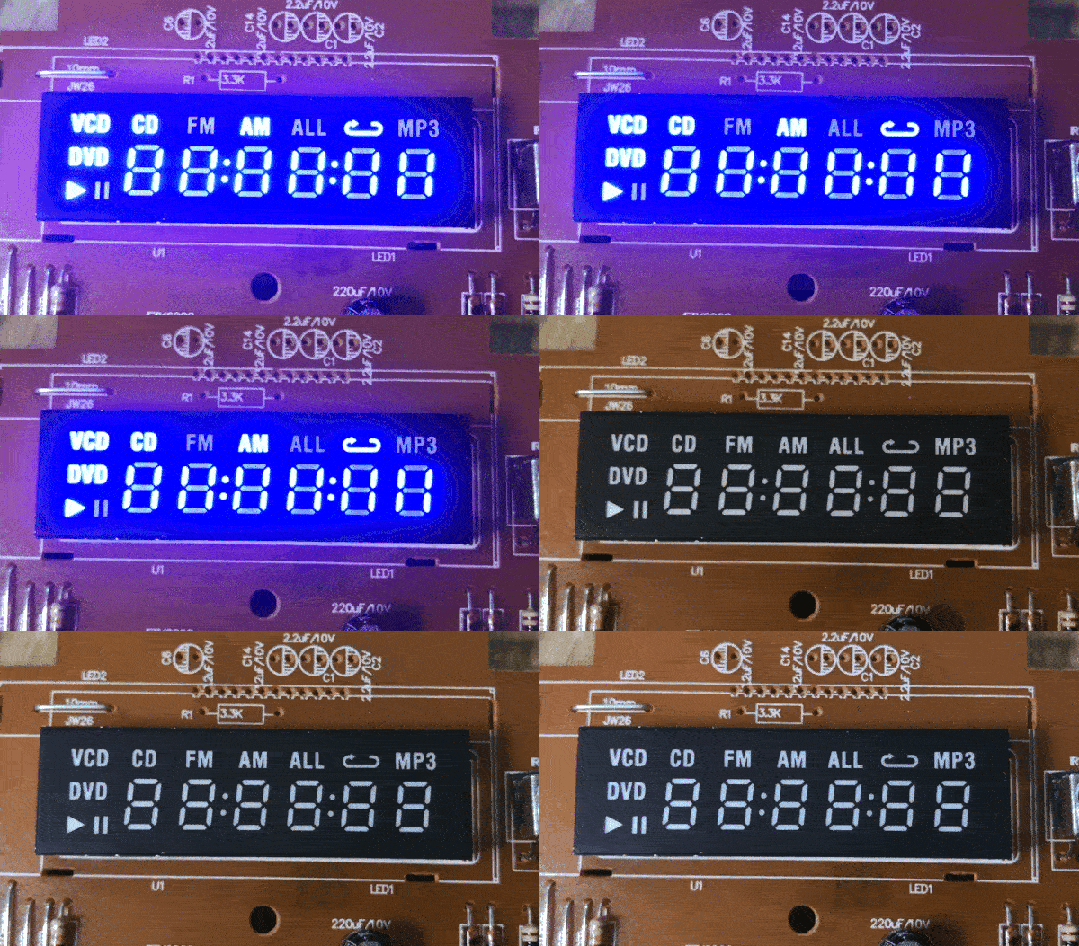
With correct configuration:
Segments
I then started experimenting with how to control the segments. It turned out that the segments of a single digit are scattered over different registers. That is, code like this:
Code: C / C++
puts out the first digit:
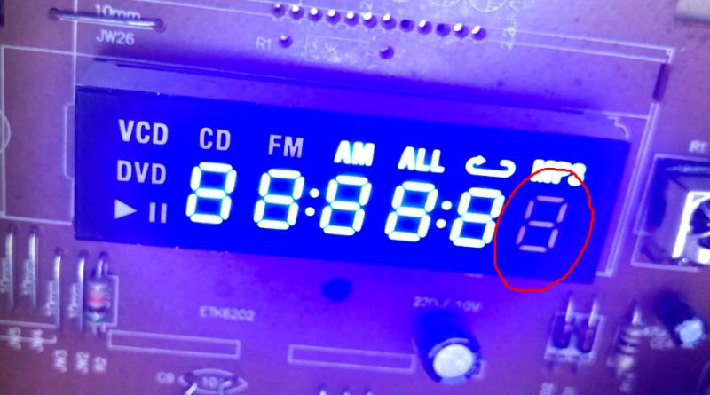
All that remains is to manually check which position corresponds to which segment - then digit masks can be created based on this.
Digits
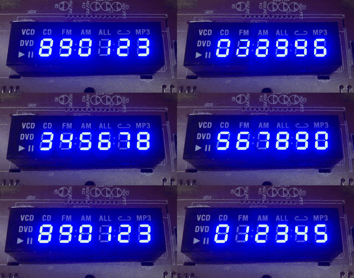
I also then identified which registers are associated with the digits at all - not all, basically every other register:
Code: C / C++
A simple scrolling of the digits is realised above.
Transform to a common buffer, icons and countdown
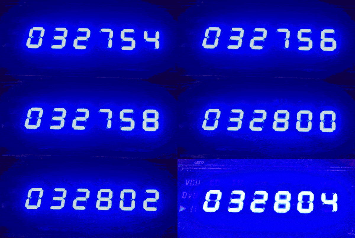
Now you could already do a normal countdown or timer, but you still need to separate the buffer so that it is shared with the icons. This is because the array that is there now represents all the segments - not just the digits themselves.
The array on is now global, and the function drawText lights or extinguishes all digit segments accordingly. Additionally i have isolated a helper function setIcon that lights or extinguishes a given segment defined by byte and bit index.
Most importantly, setIcon can be called once and subsequent drawText will not overwrite the changes.
We also managed to find both colons.
Code: C / C++
Auxiliary functions for icons:
Code: C / C++
Decode the keys.
The reading is very simple. We simply send the appropriate command and then read the data from the same pin we sent it with. The controller outputs the data on the falling edge.
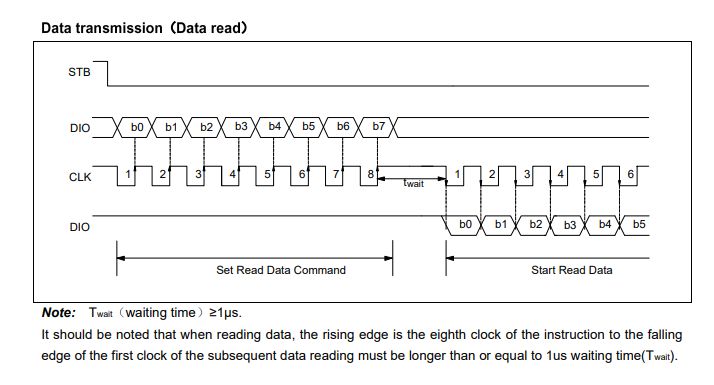
There's an interesting issue here too, because the CD1628 returns 5 bytes to us, and only selected bits of these relate to the keys - the rest are meaningless. I don't know where this design decision came from.

I've done away with specifying these bits, I just keep an array of five bytes and with each read I check which bits have changed, and then call the functions that handle the events, key press and key release separately.
Code: C / C++
Result:
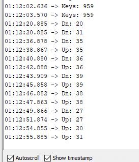
In this way you could make a functional clock or device controller with a display. You could still run an encoder and harness it too.
Summary
The equipment came to me incomplete, although I certainly know that the power supply was in working order and useful to the original owner.
In addition to the power supply there was the motherboard and front display PCB.
The motherboard turned out to be quite interesting, I was able to rip the Flash memory, determine the MCU architecture, analyse its firmware and even find its links to chips from DVD players. I also wanted to upload a simple "blink LED" to it, but unfortunately this one didn't start - I didn't experiment with it further, though, as I suspect something may have been corrupted earlier.
The front panel also caught my interest, and in this case managed to get it working easily from the Arduino. Almost all of it is realised using the CD1628 chip, a unified display and keyboard controller similar to the more popular TM1650, TM1637, TM1636, etc. Even the register addresses match.
All in all, the adventure was interesting.
I'm attaching the ripped 2MB batch, maybe someone wants to open it in Ghidra too:
https://github.com/openshwprojects/FlashDumps/commit/dae69584d40094af235c3fbebc51254746f39f4e
Cool? Ranking DIY Helpful post? Buy me a coffee.


