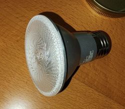
To preface this, I will probably go into more detail than is needed but, it is good for people who dont have much experiance in this realm. I will take you from disassembley all the way to final config with pictures!
This bulb has an FCC ID and photos from the FCC but, the revision 1 bulb used the 7321T chip (tuya cordcutter exploitable) while my version of the bulbs is version 3 which uses the 7321n chip. If you have firmware 1.31.21 you can use tuya cloudcutter (so dont upgrade in the smartlife app). If you have 1.5.21+ then the tuya cloudcutter exploit is unavailable.
The way I found out these were v3 was using tinytuya and getting the local key for the devices. In the tuya dump JSON files it has a string of "34869 V3". Also of note is, "sn", which holds a string which corresponds to the QR Code sticker that is on top of the 7321n chip when disassembled.
Excerpt of tinytuya devices.json:
Let's begin the disassembly:
First a photo of an undisturbed bulb:
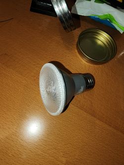
Take the Live input cap off of the bulb socket, you can use a fingernail to get under the lip to pop it up:
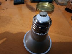
Once it is removed:
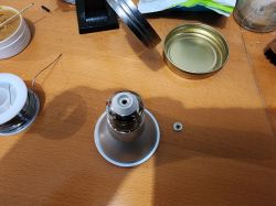
Next, take some pliers and GENTLY squeeze the bulb socket to get it to break loose from the plastic housing, I also rotated it back and forth while applying pressure.
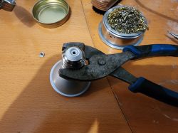
After removal of the socket:
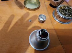
Now, we can move onto the other end of the bulb, I used a utility knife to get inbetween the lens and the body and worked my way around to pop the lens off:
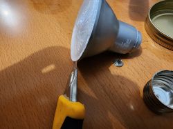
In my bulbs, there is some sort of white mastic substance used as glue to keep the lens on and hold the LED plate in place. You can also see some sort of white plastic ring that sits inside of the plastic body (for light glare perhaps?). You will need to remove that plastic ring and then remove enough of the white glue to pop the LED plate out.
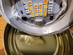
After pulling the white ring out:
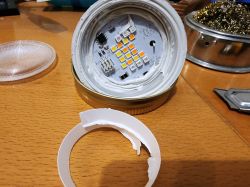
Now comes the fun part of removing the glue and popping the LED plate out. Take a flathead screwdriver or something similar and scrape as much of the white glue off of the led plate as you can. Use the screwdriver to try and pop the plate up a little bit to loosen it from the glue. Then turn the bulb over and push on the bottom PCB to pop the plate up.
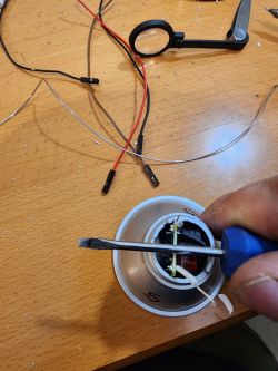
This leaves the plastic body separated from the PCB:
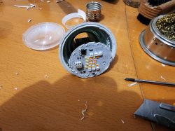
Now, lets move onto the PCB and the choice of either leaving the daughterboard in place or removing the daughter board and then resoldering it back in after flashing. I personally desolder the daughter board and then resolder it after flashing. Leaving it in place is doable but, it is a nightmare to solder the TX/RX wires in place.
PCB after removing from plastic body:
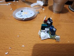
The T1/R1 pads are on the backside of the daughter board. You can see them here in the top left corner of the white PCB.
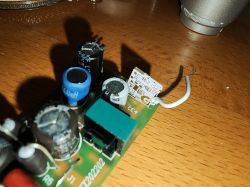
If you are soldering with daughter board in place, I highly recommend a fine tipped soldering point:
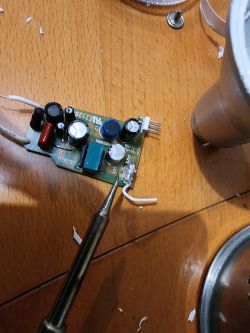
Put flux on the r1/t1 pads and then tin the pad with solder. Solder the wires on for tx/rx:
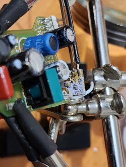
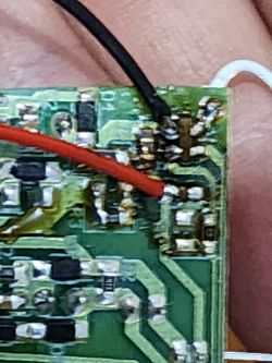
Next, get 3.3V and GND wired up. These ones are easy as the pads are much larger. You will need to solder the wires onto the main PCB.
First here is the schematic for CBLC5:
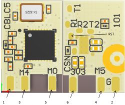
| Symbol | I/O type | Function | ANT | O | Pad pin for the external antenna | GND | P | Ground pin | M4 | I/O | Support hardware PWM and correspond to PA 24 on the internal IC | M5 | I/O | Support hardware PWM and correspond to PA 26 on the internal IC | M0 | I/O | Support hardware PWM and correspond to PA 6 on the internal IC | 3V3 | P | Power supply pin |
| Definitions of test points | Symbol | I/O type | Function | R2 | I/O | UART2_RX, LOG RX, which corresponds to P1 on the internal IC | T2 | I/O | UART2_TX, LOG TX, which corresponds to P0 on the internal IC | R1 | I/O | UART1_RX, user serial interface RX, which corresponds to P10 on the internal IC | T1 | I/O | UART1_TX, user serial interface TX, which corresponds to P11 on the internal IC | CSN | I | If connected to the ground before powered on, enter the RF test mode. If not connected or connected to VCC before powered on, enter the firmware application mode. | None | I | RST pin, which corresponds to CEN on the internal IC |
Wire up 3.3V and GND to the main PCB:
If you want to remove the daughter board and solder the wires on:
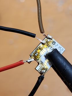
The only advice I have for soldering the wires on is to use freshly stripped, non tinned, stranded wire. If the wires are tinned or junked up, it will be hard to get it to stick to the pad. I spent an ungodly amount of time trying to solder tinned, junked up wires to the rx/tx pads and ended up tearing one of the pads off, dont be me.
I use linux so I needed to install mono before I could use the new GUIflasher tool and then clone the flasher tool repo and issue xbuild.
Time to flash!
- Now make sure your USB to Serial adapter is set to output 3.3V, 5V will damage the chip!
- Connect the USB2Serial adapter to the chip: VIN->3.3, GND->G, RX->TX, TX->RX.
- Open the flashing tool and set the port for the USB2serial adapter (ttyUSB0 in my case)
- Set the chip as 7321N (or 7321T if you have that chip)
- In the top row of tabs, you will see UART Timeouts. Go into it and set the timeouts higher. I used 10, 10, 5.
- Read the flash and backup the original firmware. Hit read flash, wait for the logs to say it is looking for the bus and then remove the 3.3 power from the chip for 1 secxond and then reapply power (I literally pulled the 3.3v wire from the serial adapter and then reinserted it)
- A dialog should pop up with JSON data to import after OBK is installed, copy the JSON data.
- If all goes well, download the most recent OpenBeken firmware using the flasher tool.
- Select the firmware to install in the flasher tool and hit "write"
- Wait for it to say its looking for bus and do the power pull again until it starts erasing and writing.
- After writing is successful, pull the 3.3V from the chip, wait 2-3 seconds and then repower it. Start looking for on OBK WiFi SSID, if you find one, the chip is flashed and working!
Now, you need to reassemble the bulb and power it up. Join the bulbs SSID and then navigate to 192.168.4.1 in a browser, this should bring you to the web interface of the bulb so you can configure it.
- In the web gui go to "Config" then "Flags". make sure flags 9, 10 and 12 are set. the main one is the ST2135: send different channels for WW and CW. White temperature wont work without that flag.
- Copy the JSON data from the reading process
- In the web GUI, click "Launch web app"
- in the web app, select "Import" from the top row of tabs and paste the JSON data into the JSON input field.
- Review the dialogs and then click the button to upload the OBK config, go back to the web gui and click "Restart".
- Start tesing the bulb to see if it toggles on/off and does RBG and WW/CW. Sometimes I needed to go into the web app > Tools > and toggle the bulb using the "100% RED/GREEN/BLUE" buttoins before the bulb would start working. If your bulb does not work even after fiddling around, you may have briodged ajoint with solder or mistakinly moved a resisitor or cap. Look on the board and see if you can find any defects and fix them.
If you did not get any JSON data from the original flash read, the 2 pins of note are 24 and 26.
Pin 24: SM2135DAT
Pin 26: SM2135CLK

LED remap:  2 1 0 4 3
Here is the generated script details:
ClearIO // clear old GPIO/channels
lfs_format // clear LFS
StartupCommand ""  // clear STARTUP
stopDriver *  // kill drivers
startDriver SM2135 // so we have led_map available
setPinRole 24 SM2135DAT
setPinRole 26 SM2135CLK
LED_Map 2 1 0 4 3
Congrats! you now have an OBK device that is local only! Enjoy!
Cool? Ranking DIY


