As part of the device interiors section in this material you will find pictures of the electronics boards of several hard drives, we will see how HDD electronics have changed over the years.
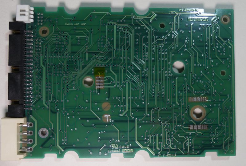
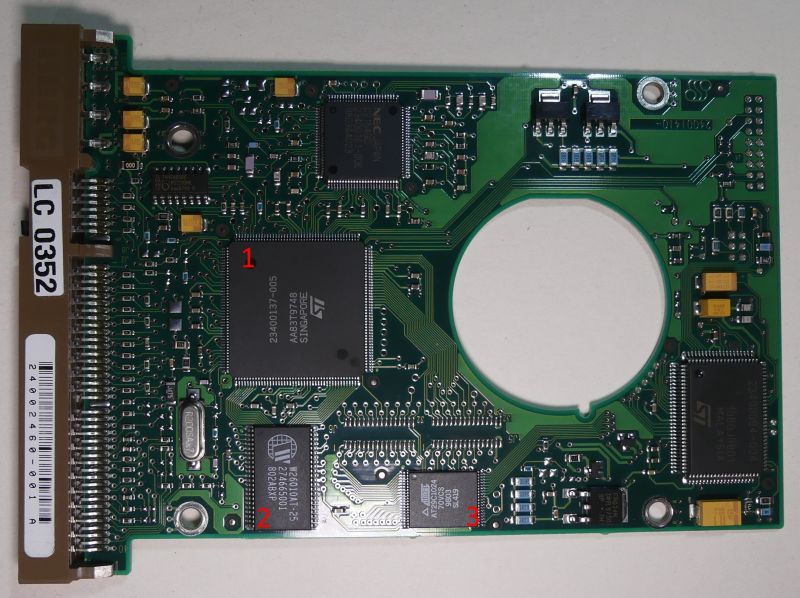
The first board is from a disk with a capacity of 40MB .
Many discrete elements can be seen.
1) parallel interface circuit
2) RAM -. SRAM 32k 8b
3) ROM
4) "power" circuit to control the platter motor
5) "power" circuit to control the heads
On the other side of the board you will find no electronic components, only the contact fields for the platter motor and the contacts for controlling the head arm and communicating with the head. This is how it will look like for all other disks.
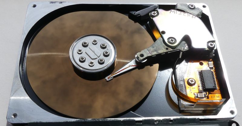
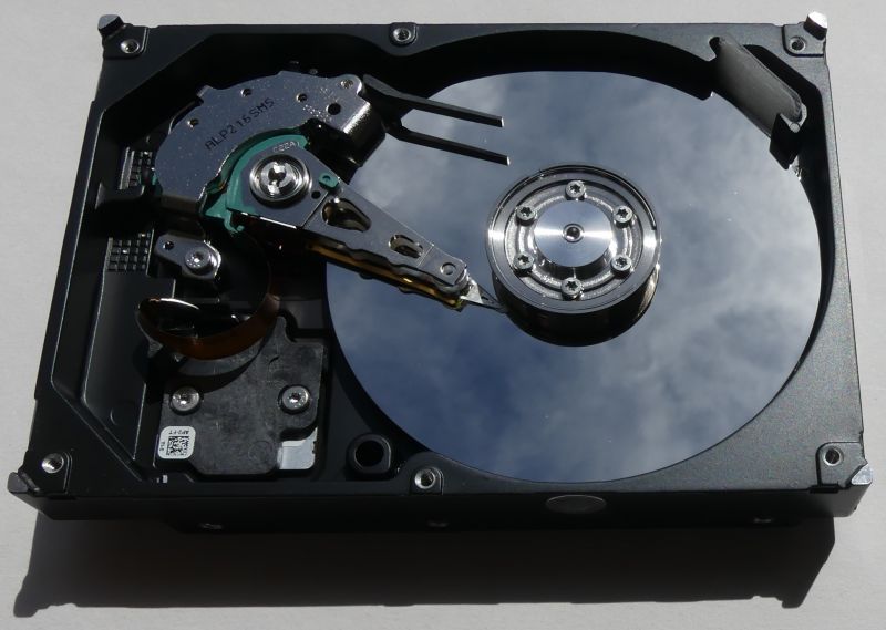
Data is stored on one platter by two heads.
In the Ultra ATA drive 4GB a greater degree of integration can be seen, such drives used to achieve transfers in the order of 4MB/s which is nowadays a bandwidth often less than the speed of an internet connection...
1) interface circuitry and arguably the drive control
2) RAM - SRAM 64K x 16b
3) ROM
The rest of the circuitry is the control of the motor and head arm and the processing and generation of signals for the heads.
Two platters and four heads.
W 40GB drive with ATA133 interface we see a further increase in the scale of integration. Such drives provided transfers up to 10x faster than the 4GB predecessor.
1) interface chip and disk controller
2) RAM - SDRAM 512k x16b
3) power chip
One platter two heads.
One disc.
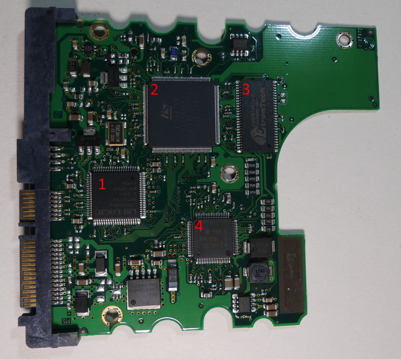
Disk 80GB changed to serial SATA interface.
1) interface circuit
2) disk controller
3) RAM - SDRAM 1M x 16b x 4 banks
4) 'power' circuit.
One plate and two heads.
.
Drive 80GB Newer generation SATA, further scale-up of integration is evident. Gone is the separate interface chip, now the disk controller chip is connected to the SATA interface. In this version, the electronics have moved to the side where the contact fields for the platter drive and head arm and the signals for the heads are located.
1) controller
2) RAM - SDRAM 1M x16b x4 banks
3) 'power' circuit
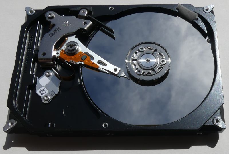
One platter and one head.
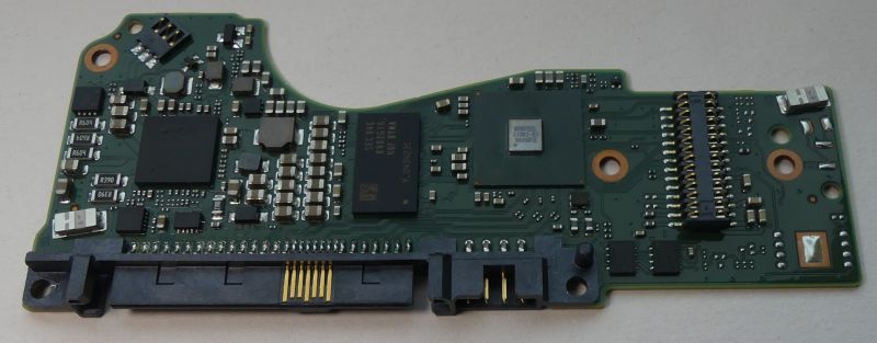
Disc. 10TB a drastic reduction in the size of the electronics board can be seen.
Why are there still 3 main circuits on the PCB?
I suspect, that the "power" chip is made in a different process/lithography than the disk controller, as is the RAM, and it still pays to put two separate chips. RAM in a separate module is perhaps an easy production model with a different amount of cache?
Today most of the media we use do not contain spinning platters, HDD are displaced by FLASH memory.
Have you come across any interesting media designs
or any design details of interest to you in the pictures in this material?
If you prefer footage, below are attempts to identify the circuits used in the first of the 40MB HDDs:
And the operation of the newer HDD with SATA interface:
The helium-filled drives are sealed like a can of canned food
Cool? Ranking DIY


