Hello! This is my first post in this forum section, so please bear with me :)
I was motivated to write this article by a post by user p.kaczmarek2, located here:
https://www.elektroda.pl/rtvforum/topic3692552.html
He presented the operation and construction of a cheap USB hub, i.e. Chinese, which did not impress with either quality or design solutions. Unfortunately, there are more and more such devices, and people buy cheaper ones and do not pay attention to more expensive and better devices according to the principle "If it works, don't touch it!"
In today's presentation, he will be the hero HUB TP-LINK UH720 . It is a splitter operating in the USB 3.0 standard. In addition, there are two fast charging ports and a power switch for the device.
I will not focus on tests (which does not mean that I will not do any), because the operation of the USB hub is rather the same in every case and it can be simply boring. Let's start!
PRESENTATION
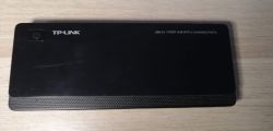
The device (or rather its housing) is made entirely of black plastic. The top surface containing the power button and logo is smooth and shiny. It was not a good idea on the part of the manufacturer, because EVERY, even the smallest scratch can be seen on the shiny housing.
The second part of the upper shell is directly above the ports. It is slightly perforated, thanks to which the windows for the LEDs are perfectly integrated and can only be seen when they are lit.
Before someone writes: "But you could at least clean this HUB...". I answer: my copy is three years old and does not look good anymore (scratches), in addition, even the smallest dust particles can be seen on the housing. I cleaned it 3 times before shooting... It didn't turn out very well, but I'm happy to show it to you anyway.
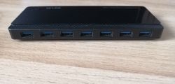
From the front we see 7 USB 3.0 ports. Simply.
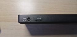
On the back (because it is an active HUB), in addition to the USB micro B socket, there is a 12V power socket.
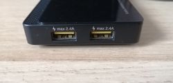
On the right side - a nice addition - 2 fast charging sockets with a maximum current of 2.4A (not connected by bus to the computer)
Two pieces of rubber are glued to the bottom to prevent slipping.
KIT ELEMENTS
In the set we get:
► TP-LINK UH720 USB 3.0 hub
► Power adapter
► USB 3.0 cable
► Instruction
TESTS
When I said there wouldn't be many, I wasn't lying. Here they are:
1. Passive power, USB 3.0
Connected to the hub:
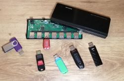
- 6 portable FLASH memories
- additional hub 2.0
- mouse
- chinese memory card reader
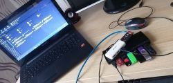
"This PC" view:

Device manager:
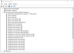
Further loading caused a reset of all devices connected to the hub, and the system displayed the appropriate message:

2. Power on, USB 3.0
Now, in addition to the things above, I was able to connect a hard drive, one additional memory (small hub 2.0 gave up and did not power any more) and charged two phones via the charging sockets.
3. Does the hub reduce the transfer speed?
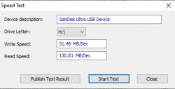
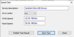
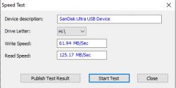
flash memory (tested in USBDeview):
| Test | Record | Reading |
| Control sample (memory directly in the USB port of the computer) | 31.48MB/s | 130.81MB/s |
| HUB without external power | 16.55MB/s | 30.00MB/s |
| HUB with external power supply | 61.94MB/s | 125.17MB/s |
If the pictures appeal to anyone, please let me know
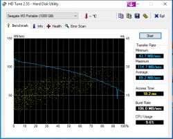
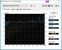
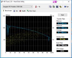
Portable hard drive (tested in HDTune):
| Test | Minimal transfer | Maximum transfer | Average transfer |
| Control sample (memory directly in the USB port of the computer) | 43.7 MB/s | 114.7 MB/s | 89.2MB/s |
| HUB without external power | 20.5MB/s | 33.1 MB/s | 26.0MB/s |
| HUB with external power supply | 44.8MB/s | 114.7MB/s | 88.7MB/s |
Transfer speed graphs and detailed information...
I decided to leave the test results to my own interpretation. :D
INTERIOR
Now for something you've all been waiting for! Time to open the case!
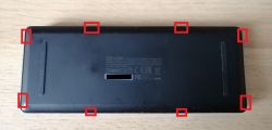
It's not very complicated to open, but it does require a bit of fiddling with the snaps.
The device opens from the bottom. I recommend to equip yourself with a special plate for opening - it leaves less traces.
We push it into the latch and pry it up.
Attention! I do not recommend screwdrivers, probes or knives! - they leave a lot of ugly marks and burrs!
Fortunately, the latches are thick and strong, so they have no chance of breaking when gently unfastening them.
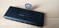
Snap Map:
After removing the shell, the motherboard appears, which fills all the available space.
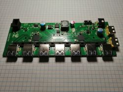
The album itself can be divided into 4 sections. I marked them with the letters A,B,C,D.
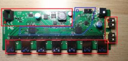
A - power section
B - 7 USB 3.0 ports
C - charging ports
D - support for USB ports
Now I will break down the individual sections:
Power:
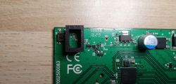
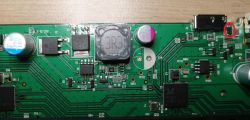
Power goes to the GH15B stabilizer. It is actually AZ1117 (note in the attachment) in the ADJ version, set with resistors R8 and R9 (10Ω and 30Ω respectively
This voltage is probably supplied by a tiny U4 chip, which together with the transistors is responsible for switching the whole device on and off with the SW1 monostable button and controlling the D1 LED. There is a sponge around it to stop the light within the button.
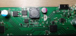
Then the integrated circuit of the main pulse converter built on the APW8720B system is powered (note in the attachment).
There is also a coil, smoothing capacitors and two large MOSFET CED3172 transistors (note in the attachment).
The converter produces a high-current 5V voltage that powers all USB ports.
USB 3.0 Ports:
An interesting fact about them is that each is protected by a separate fuse.
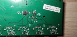
Charging Ports:
Contrary to appearances, it is more than a port connected to 5V. The data lines are routed to a tiny but nifty U34 chip labeled 3004. I haven't found any information about it, but it might be something like the TPS2513. The system informs the charged device about the charging method.
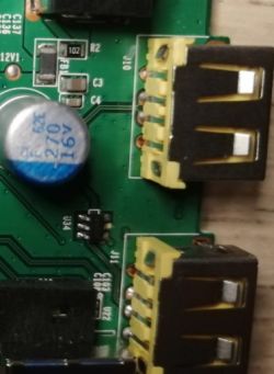
Link to an interesting article on the subject here
USB port support:
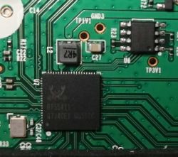
The whole thing is supported by two RTS5411 integrated circuits (note in the attachment). Each of them can handle 4 USB ports. So where did the eighth port in the hub go? It was used to connect the systems with each other. Therefore, the operating system detects the entire device as 2 hubs.
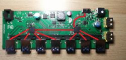
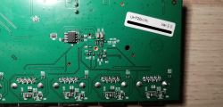
Next to each processor we see a chip in a silver casing. It is a quartz generator clocking the RTS5411 chip with a clock frequency of 12MHz. In addition to them, we can also see a flash memory for the SPI interface containing procedural software (firmware). The second bone is on the bottom of the plate.
A WORD OF CONCLUSION
It is a really good device. I recommend them to anyone who has some USB devices and a limited amount of ports on their favorite device.
Just remember to power it up :)
Minuses?
► The factory power supply is EXTREMELY loud and very clumsy. I recently replaced it with a more powerful 12V/5A power supply.
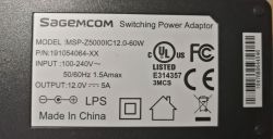
Unfortunately - after this operation I had to buy and solder a new DC12V socket because that one had too small a pin inside and did not make contact.
► The USB cable included in the set is of good quality, but I recommend getting a spare one, because the micro USB B plug broke in mine after two years
► the housing scratches terribly
I guess I can end on this. I hope you liked this article. As promised - all the notes are in the attachments.
In addition, I provide a file with the firmware for the RTS5411 chip (in HEX notation marked with the year 2015 - available on the Internet is marked as 2014).
ATTENTION!
I do not recommend using update programs, because they are designed to update only one chip at a time (the second one will remain outdated, which can lead to numerous errors in the operation of the device). The only way is to desolder both bones and program them with a memory programmer (e.g. CH341A).
If I forgot something or made a mistake - write.
Greetings to all readers!
Cool? Ranking DIY


