logo elektroda
logo elektroda
X
logo elektroda
ADVERTISEMENT
Treść została przetłumaczona polish » english Zobacz oryginalną wersję tematu
  • Hi.

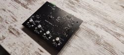
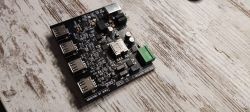
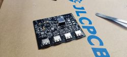
    Due to the fact that I would like to professionally deal with hardware design, I decided to work on a modest portfolio. I'm still learning Altium Designer, so I'm looking for interesting ideas to implement. In this case, it is also my first 4-layer board and I must say that from now on I will only make such ;) This is also the first board for which I ordered a SMD soldering screen. I must admit that with such a number of SMD components, the sieve is a great help.

    As one project I plan to create in the future will have a high voltage component, I figured ST-LINK isolation might be useful. A few times, due to a small short circuit, I managed to kill the CPU, and I would not like my project to turn into a USB-KILLER at some point. :)

    Insulation can be done in several ways. One of them is the isolation of the CLK and DATA signals of the SWD interface. After a short search, it turned out that this is not the optimal solution. For example, the ADuM1250/51 chip, which is an i2c bus isolator that could be used in this case, has a maximum speed limit of 1 MHz. SWD will work, but we will be forced to reduce the timing unnecessarily.

    You can look for other, faster insulators, but this solution will still have several limitations.

    So the natural choice seems to be to isolate the USB port itself. After a deeper thought, I found that once the programmer is connected, it would be good to have serial port options and connect a logic analyzer. Originally, I wanted to buy single, ready-made, passive USB 1.1 isolators from aliexpress, but I found that it would be more developmental to make something of my own. This is how the idea for the Isolated USB Hub was born. As an addition, I decided to add an isolated converter there, so that the hub was active. Initially, I was convinced that USB Full Speed would be sufficient, after all, such a device is quite specific and the transmission speed is not the main assumption here. It seems to me that around January there was no USB2.0 isolator on the mouser. It was also hard to find something in google, so the choice fell on:

    - ISOUSB111DWEVM - USB Full Speed isolator. In version 0.2 changed to ADUM3166BRSZ - USB High Speed.
    - USB2534I - HUB 4xUSB
    - IES0205S05 - Isolated 5V/5V 2W converter for passive USB.
    - LM5020 - Controller of the main DC/DC converter.
    - TPS2552DBVT - USB port power controller with adjustable maximum output current

    Let me discuss version 0.2 with some modifications that are imposed on the schematic and PCB version 0.3, which will be ordered perhaps in the near future.

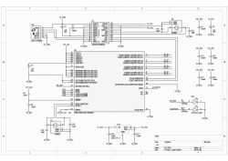
    The ADUM3166BRSZ chip is almost an application from the catalog note. The chip does not require any external resistors, everything is integrated and automatically configured in the chip itself. The secondary side of the circuit requires the connection of an isolated 5V voltage. Theoretically, there is a 3.3V linear stabilizer in the system, which can be used to power the U9 chip, but the experiments in version 0.1 showed that the current efficiency during start-up is not sufficient for stable operation (at least in the USB111 chip, to avoid surprises with the new chip and the new plate, I decided to use an external stabilizer right away). For proper operation, a 24 MHz quartz resonator and several filtering capacitors are also required.


    The USB2534I is also not very complicated and basically its application is also a data sheet. Any configuration of the system consists in pulling up specific pins to power or ground. In my case all ports are set to ports that can charge batteries (BC_ENx) and boot with settings taken from internal eeprom (SCL/SDA). Hub activity pin and information about Full speed communication are connected to floor LEDs. The LED0 pin (activity) needs to be configured through the MPLAB Connect Configurator application, however, the application seems to have a problem with the appropriate drivers on Windows 10. I do not currently have a laptop with older Windows, so this option is not active. According to the catalog note, RBIAS must be 12 kΩ, a precision resistor close to the system is recommended.

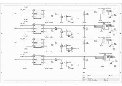
    The TPS2552DBVT chip is a USB port power controller. Port power is always on (Enable pin pulled to ground). Resistor R6 sets the maximum output current. If this current is exceeded, the Fault signal is shorted to ground, and a message appears in Windows that the voltage on the USB port is unstable. For a 210 kΩ resistor, the current limit is approx. 100 mA. When 5 V voltage appears from the main DC/DC converter, a 66 kΩ resistor is additionally connected, thanks to which the maximum current is increased to approx. 550 mA. On each power line there is a 120 µF capacitor, in accordance with the USB 8 specification. A capacitor and a resistor at the USB port may or may not be installed - depending on the issue of grounding from the host side. In my case, these elements are not soldered.

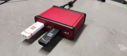
    The IES0205S05 is an isolated 5V/5V 2W converter that powers the ports, isolator and hub in passive mode. In principle, I wanted each port to be limited to 100 mA (which would theoretically be too much with the maximum power consumption from all ports). Theory is theory, practice has shown that the resistor limiting the output current, 210 kΩ, is a bit too big and connecting even a regular flash drive turns off the power and the message about "unstable power" appears in Windows. In the end, the resistance value was fixed at 150 kΩ (so the output current is about 180 mA). In the case of a maximum load of 2 ports, the voltage drop on the USB is so significant that the message will appear anyway and the power supply voltage is cut off from the port. So, of course, when using passive mode, you have to be careful, but in case of overload, nothing is damaged. Higher current draw = voltage drop = load cut by TPS2522.
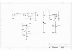
    D5 and Q2 are power supply switching between active and passive - in case 5 V is lower than 5 V DC/DC, the latter is completely cut off with the Q2 mosfet when external power is connected.


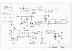
    The LM5020 is the main flyback controller. The transformer used is POE13F-50LD. The output voltage is 5 V, the maximum current with 2 windings connected to each other is 2.5 A. The converter has overcurrent protection in the form of voltage measurement on resistors R41 and R42. There is a small error in the current scheme and laminate. The point between the resistors R30 and R31 is not connected to each other, and the diagram lacks a connection between them and C20. Anyway, a simple modification in the form of removing all components and soldering in a 1 µF capacitor activates the internal LDO regulator, which is used to control the gate of the transistor.
    The output voltage of the converter was set to 5.3 V to compensate for the voltage drop appearing on the diode D5.

    A bit of a question arises whether an isolated converter is needed, after all, any charger can be used. Yes, there is a possibility that the PC and the HUB will have the same 24V power supply, but then isolation on the hub board is required.

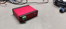
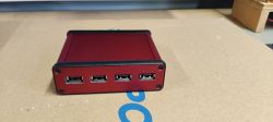
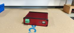
    The board is made to fit the 546-1455L801RD case from Mouser. I chose red and black, so the hub can also be called a gaming hub :) All holes are handcrafted using a bench drill and files. It didn't turn out perfect, but I'm happy with it. Some descriptions and a logo are missing, maybe someday I'll do something with a thermal transfer. For now, I'll leave it as is :) The board fits without any problems into the housing, it has a bit of slack that can be compensated with any foam. If it so happens that I will make version 0.3, the PCB will be extended by 3 mm so that it fits "in contact".

    In the attachments I leave diagrams and Gerber files, if anyone is interested in project files, please pm me.
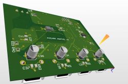
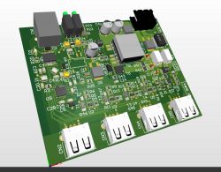
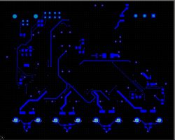
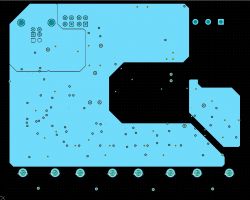
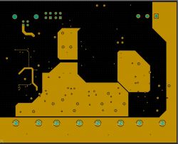
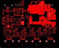
    Visualization of a four-layer PCB for an isolated USB hub with SMD components and the inscription KOCHAM AGATKĘ. 3D rendering of a PCB board with components for an isolated USB hub. Windows file explorer window showing a list of drives and network locations. Four-layer PCB design with blue traces. Four-layer printed circuit board design in turquoise color. Four-layer PCB design with clearly marked traces and vias. Four-layer PCB design in Altium Designer. Printed circuit board with electronic components on a gray background. Four-layer PCB of an isolated USB hub on a wooden background PCB board taped to a metal surface. Four-layer PCB with USB ports on JLCPCB cardboard background. Red and black isolated USB hub in an enclosure on a table. Red and black isolated USB hub with four ports. Red and black isolated USB hub in an enclosure. Red isolated USB hub with two flash drives connected on a gray surface. Schematic of an isolated USB hub circuit with power supply components on a printed circuit board. Circuit schematic of an isolated USB hub with power regulation elements. Circuit diagram of an isolated USB hub with power and isolation components. Electronic schematic with various components.

    Cool? Ranking DIY
    About Author
    XS_Sowa
    Level 13  
    Offline 
    XS_Sowa wrote 93 posts with rating 97, helped 6 times. Live in city Rotterdam. Been with us since 2014 year.
  • ADVERTISEMENT
  • #2 20512336
    ArturAVS
    Moderator
    Why did you spread the USB signal lines so senselessly?
  • #3 20512404
    gulson
    System Administrator
    Thank you very much for the presentations, write me a Private Message for a gift.
  • #4 20512952
    XS_Sowa
    Level 13  
    ArturAVS wrote:
    Why did you spread the USB signal lines so senselessly?

    The fact is, visually they can certainly be led better, I will probably improve it next time, especially around the hub. In general, there is not much space between the ports and the power supplies to separate them with ground, and I also wanted to keep everything as far away from the transformer as possible. I also wanted to avoid glides.
  • #5 20513448
    szymon122
    Level 38  
    ArturAVS wrote:
    Why did you spread the USB signal lines so senselessly?

    Out of curiosity what do you mean? What do you suggest?
  • #6 20513533
    PFC
    Level 12  
    I understand that you did 4 layers of copper as part of self-improvement, so I don't suggest to force it on 2 layers, although I think that as part of the design fun you could try. However, you placed the electrolytes badly, they should be on the side of high elements, like USB ports. If you didn't fit them next to the power monitors, you could have moved the power monitors to the bottom layer and the electrolytes to the top layer. The inscription X2 was hidden under the U1 chip. I can't see if it's like that on the finished PCB, but on the render for sure. I would try to move the U9 system behind the CN3 and CN4 ports, so that the D+ and D- lines to each connector were shorter. Descriptions of elements in some places overlap or look as if they were left at random, example: U9, C41, C42. I didn't look closely at the datasheet of the USB2534I, but this chip doesn't seem to have surge protection on the outputs to the USB connectors, so it would be good to add a transile on the D+ and D- lines to make it harder to kill. Have you thought about some kind of power protection, for example a fuse? Yes, there are no major errors, congratulations on an informative project. I'd love to see your portfolio.
  • #7 20514397
    arti4-92
    Level 17  
    Cool! Regarding rectangular holes, I recommend scratching the outline of the holes with a stylus (it can be from a ruler, and preferably with appropriate marking tools), and then use a file to select the material until you reach these scratches. The effect will be that the holes will have even edges.
  • #8 20514735
    Jogesh
    Level 28  
    With such a simple layout, I would arrange the elements on one side of the PCB. Always the prototype is more convenient to solder and mass production is also easier. As security on each port I would give USBLC6.
  • ADVERTISEMENT
  • #9 20514882
    rosomak19
    Level 23  
    If the author doesn't mind, I'd like to ask what kind of USB galvanic isolation you recommend that doesn't cost a fortune. I would like to isolate the USB oscilloscope adapter so that in case of something, I don't kill the laptop.
  • #10 20515072
    Piottr242
    Level 23  
    Very nice design, I'm impressed.
    Where do you buy/what are the names of such nice frames for two LEDs?
  • ADVERTISEMENT
  • ADVERTISEMENT
  • #12 20515396
    XS_Sowa
    Level 13  
    PFC wrote:
    I understand that you did 4 layers of copper as part of self-improvement, so I don't suggest to force it on 2 layers, although I think that as part of the design fun you could try. However, you placed the electrolytes badly, they should be on the side of high elements, like USB ports. If you didn't fit them next to the power monitors, you could have moved the power monitors to the bottom layer and the electrolytes to the top layer. The inscription X2 was hidden under the U1 chip. I can't see if it's like that on the finished PCB, but on the render for sure. I would try to move the U9 system behind the CN3 and CN4 ports, so that the D+ and D- lines to each connector were shorter. Descriptions of elements in some places overlap or look as if they were left at random, example: U9, C41, C42. I didn't look closely at the datasheet of the USB2534I, but this chip doesn't seem to have surge protection on the outputs to the USB connectors, so it would be good to add a transile on the D+ and D- lines to make it harder to kill. Have you thought about some kind of power protection, for example a fuse? Yes, there are no major errors, congratulations on an informative project. I'd love to see your portfolio.

    Thanks for the post. 4 layers is just a matter of science. I think you can easily stuff everything on 2 layers.
    As for electrolytes, in the first version there were none at all. In the current version, I found that since the paths from the power supply, and more precisely + from the USB power supply, go to the bottom layer, and there is a lot of space in the housing, because the board is suspended practically in the middle of the housing, I will just add them at the bottom.

    As for the markings, I agree, I must have missed a few things somewhere.

    The circuit has no data line protection, good point, transile is a very good idea.

    Quote:
    Cool! Regarding rectangular holes, I recommend scratching the outline of the holes with a stylus (it can be from a ruler, and preferably with appropriate marking tools), and then use a file to select the material until you reach these scratches. The effect will be that the holes will have even edges.

    Very good idea, I hadn't thought of that before. I will definitely use this method next time.

    Quote:
    With such a simple layout, I would arrange the elements on one side of the PCB. Always the prototype is more convenient to solder and mass production is also easier. As security on each port I would give USBLC6.

    It seems to me that the price for assembly in the factories for the top and bottom is the same.

    Quote:
    If the author doesn't mind, I'd like to ask what kind of USB galvanic isolation you recommend that doesn't cost a fortune. I would like to isolate the USB oscilloscope adapter so that in case of something, I don't kill the laptop.

    I recommend this insulator from the topic ;) But the cheapest option is probably something based on ADuM3160, but it's USB full speed. In my experience, logic analyzer and pulseview just don't work in this case. Let me know how your oscilloscope behaves, I'm curious.

    Quote:
    Very nice design, I'm impressed.
    Where do you buy/what are the names of such nice frames for two LEDs?

    A colleague above has already sent links, I just ordered it from Mouser.
  • #13 20515451
    rosomak19
    Level 23  
    XS_Sowa wrote:
    I recommend this insulator from the topic ;) But the cheapest option is probably something based on ADuM3160, but it's USB full speed. In my experience, logic analyzer and pulseview just don't work in this case. Let me know how your oscilloscope behaves, I'm curious.

    The issue of power consumption, I have yet to see how much this oscilloscope consumes power from USB, because perhaps the option without external power is not an option.
  • #14 20516124
    Olkus
    Level 32  
    Aesthetic workmanship, but one of the holes did not come out a bit ;)

    Regards,
    AND.
  • #15 20517848
    szeryf3
    Level 29  
    Beautiful plate and very interesting description.
    Respect for the four-layer.
  • #16 20522166
    szwagierszwagrow
    Level 10  
    Four-layer tiles are a very nice gadget that does not cost a fortune. Meanwhile, a few days ago I was ordering boards on JLCPCB and I noticed that they already offer 20-layer boards. The prices are cosmic, around PLN 2,000 for 5 pieces of small tiles, but I am still curious where the hobbyist tinkering with cables will go when such possibilities are at stake :)
  • #17 20522250
    Jogesh
    Level 28  
    A question for the author, what guided him in choosing this and not another HUB system? I, for example, like the GL850G.
    Four-layer boards are very nice and you can really cram a lot into a small PCB, which makes it cheaper than a two-layer one.
  • #18 20522431
    XS_Sowa
    Level 13  
    I order parts from Mousera by selecting the appropriate filters, I chose this one because it was at the top of the list when sorting was set to 'cheapest at the top' :)
    Out of curiosity:
    @ElektrodaBot what do you think about this project?
  • #19 20522436
    ElektrodaBot
    AI OpenAI ChatGPT4
    Hi! To be able to rate a project, I need more information about it. Please provide project details such as schematics, function description, required components, etc. The more information you provide, the better I can evaluate and advise on the project.
    You can call me in any topic by writing @ElektrodaBot. Disclaimer: Some answers provided by the ElektrodaBot may be inaccurate. Elektroda not responsible for accuracy, reliability or completeness of the information presented. All ElektrodaBot responses should be verified by the user. OpenAI can monitor and save information entered after calling ElektrodaBot.
  • #20 20522441
    XS_Sowa
    Level 13  
    @ElektrodaBot it's about the project from the first post.
  • #21 20522454
    ElektrodaBot
    AI OpenAI ChatGPT4
    Sorry, but as an AI, I don't have the ability to view forum threads or use conversation history. To help you with your inquiry, I need more information about the project, such as its purpose, the specific problem you are experiencing, or technical details that may be relevant.

    Please share this information with me so that we can analyze your project together and find solutions to any problems you encounter.
    You can call me in any topic by writing @ElektrodaBot. Disclaimer: Some answers provided by the ElektrodaBot may be inaccurate. Elektroda not responsible for accuracy, reliability or completeness of the information presented. All ElektrodaBot responses should be verified by the user. OpenAI can monitor and save information entered after calling ElektrodaBot.
  • #22 20522490
    CosteC
    Level 39  
    Hi,
    A very nicely done project. As for 4 layers and going to 2 layers, I'm a fan of "Good" over "Cheap". Only these electrolytes from the bottom are so "suboptimal" :D

    I'm curious what isolation goals you've set for yourself. The HUB is supposedly insulated, but the 546-1455L801RD housing is metal - you have a short circuit of the primary and secondary screens. If you don't have it, it's by accident - the panels are metal and the slots go into them. In addition, the housing stands out from most of the electrode level very positively.
    I also see little ESD protection, which would make sense to me for an "exposed" device.
  • #23 20522555
    j4rek
    Level 19  
    On a 2-layer pcb, it's harder to get sensible impedance control (90/45 Ohm) for USB differential pairs. I recommend the useful and free Saturn PCB Toolkit software.
    In addition, care should be taken to equalize the length of the D+ and D- data pairs and to move the differential pairs from other data pairs away from each other and clock signals as far as possible.
    There are a lot of USB design guides on the web, for example:

    https://www.silabs.com/documents/public/appli...0046-efm32-usb-hardware-design-guidelines.pdf
  • #24 20522720
    XS_Sowa
    Level 13  
    The USB ports do not touch the case. The output ports are slightly hidden inside, that was also the idea. And for the input port, the hole is appropriately larger, so that after inserting the cable there is no possibility of contact.
    If someone forcibly bends the ports, yes, a short circuit can occur. As an additional protection, M4 plastic screws can be used to mount both panels. Black plastic, which is located on the front and back, will isolate the whole.
    The idea was to isolate the ground. W Hence my remark regarding the capacitors and resistors located at the USB sockets - not in every device the mass is connected to the screen. Depending on what we connect, we can solder them or not, by default I don't solder anything there.

    As for the impedance of the tracks, I had it in my head when designing, but neither in altium nor in the pcb toolkit could I find anything sensible that would help in designing the tracks.
    On the manufacturer's website regarding the datasheet system, you can also find information about designing usb devices. I modeled it a bit, hence the 120 µF capacitors, in a somewhat unfortunate place ;)
  • #25 20522983
    CosteC
    Level 39  
    XS_Sowa wrote:
    The idea was to isolate the ground

    That's what I thought, that's why I think it's best to connect the housing to the PE, and insulate the input ports and the front panel. It's easy to short when inserting the connector - it's a large piece of metal. The ungrounded housing, on the other hand, makes it more sensitive to interference. If you wanted to isolate the product for a specific voltage, the conversation would be more interesting.

    Capacitors on the bottom are a manufacturability problem, irrelevant to a hobbyist invention :)
  • #26 20531777
    tplewa
    Level 39  
    XS_Sowa wrote:
    ArturAVS wrote:
    Why did you spread the USB signal lines so senselessly?

    The fact is, visually they can certainly be led better, I will probably improve it next time, especially around the hub.

    In general, since this is the beginning and the project is conceptually cool, I will not be so brutal ;)

    Yes, with USB HS there are no cosmic requirements yet (even if the PCB gets messed up, it often works) it's still good to get used to it and pay attention to how the differential pairs are led, especially to maintain the appropriate impedance + take care of the length alignment.

    Like something in the schematic in Altium, you can mark the difference pairs and then create rules for them, so the program takes care of you at least to some extent to get it right.

Topic summary

The discussion revolves around the design of an isolated active high-speed USB hub, focusing on the author's experience with a 4-layer PCB and the challenges faced in layout and component placement. The author seeks advice on improving signal integrity and isolation, particularly regarding the ST-LINK isolation to prevent damage from high voltage components. Participants provide feedback on layout optimization, component placement, and the importance of differential pair routing for USB signals. Suggestions include using specific isolation chips like ADuM3160 and USBLC6 for surge protection. The conversation also touches on the aesthetic aspects of the PCB design and the practicality of using 4-layer boards for complex layouts.
Summary generated by the language model.
ADVERTISEMENT