Hi,
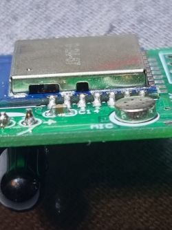
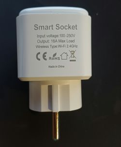
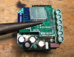
Here are some pics and some of my findings.
Luckily I have two of these devices, so I desoldered one of them.
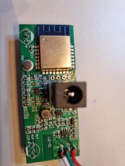
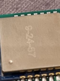
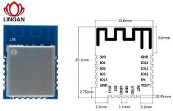
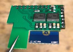
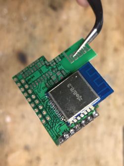
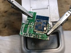
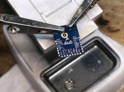
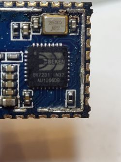
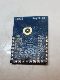
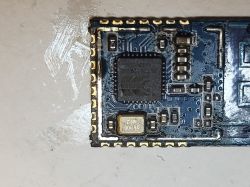
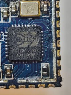
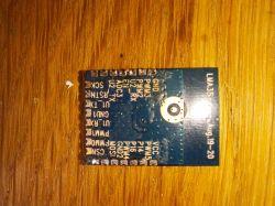
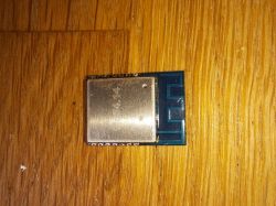
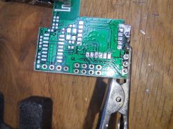
First LMA35


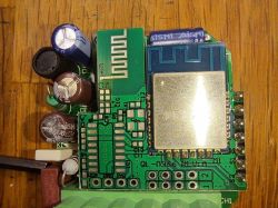
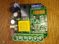
Top board


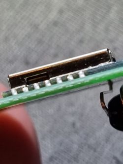
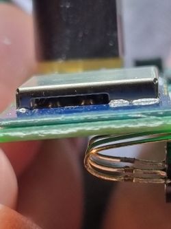
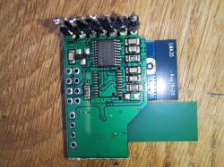
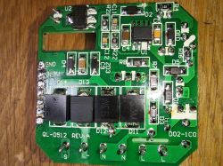
Bottom board


My Findings
Pins on LMA35 that are in use are: VCC, GND, PWM0, U1_TX
U1_RX goes to the unpopulated area (I guess this is for RF), and is not in use.
The IC on the underside of this card, I found to be 8S003F3P6 and is some kind of processor.
TX pin on LMA35 is connected to 8S003F3P6 pin RX (on the underside)
PWM0 is connected to 8S003F3P6 on pin 8 (VDD) and through the pin header to bottom board. There it is connected via some resistor and a transistor to the switch input.
PWM1 seems to be used when there are two dimmers.
I did some trace on the pin header that goes between the two boards (from the top):
Pin1=GND
Pin2=VDD(on IC on the underside)
Pin3=PC3 (on the unpopulated spot underside)
Pin4=PC3 (on 8S003F3P6)
Pin5=Q1(transistor marked P1 on the underside)
Pin6=PWM0
Pin7=PWM1
I only traced I did on the bottom board is PWM0 to the switch
My conclusion is that it somehow seems to only use TX to send data. And use PWM0 as an input. The device knows if it is on or off, so some data must be sent back to the LMA35. This is well above my knowledge, and I have no idea how this could work.
I have flashed LMA35 as a bk7231T and tried the web app to do some testing with no result. I also flashed with esphome and tried some TuyaMcu code but no result, so now I am back to openbeken again.
I'm all out of ideas and appreciate any possible info.
/Daniel
