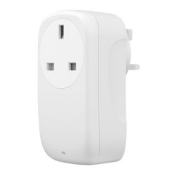
Here I'll document my findings with the BroadLink SP4L-UK smart wi-fi plug with 3-pin UK socket. I'll provide details about the BL3335-P module found inside and how this module, as it is configured in this plug, can be flashed with opensource replacement firmware OpenRDA5981.
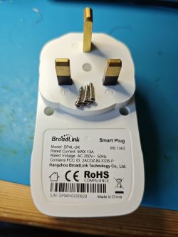
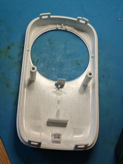
Opening begins with the removal of the 3 triangle-head screws on the underside. These hold the main case together and the plug cover plate in place.
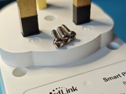
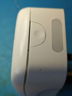
I removed the plate around power pins and used a spudger to prize open the case. Note the position of the clips. It's quite easy to break those with too much force in the wrong locations.
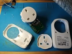
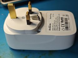
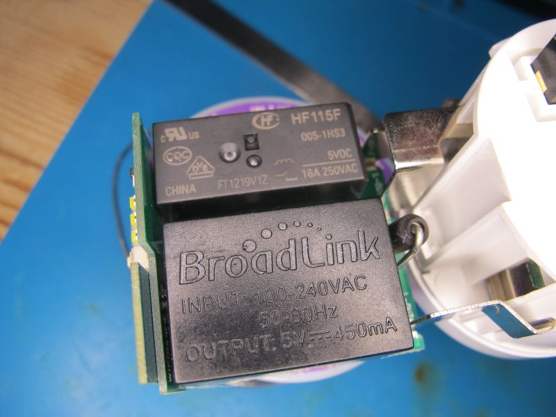
Inside we see the BroadLink 100-240VAC -> 5V DC power module alongside a Hongfa HF115F 005-1HS3 miniature electromechanical high power relay with a contact rating of 16 A at 250 VAC.
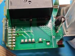
On the other side is found the mains AC and Ground planes, a silkscreen label of "SocketBoard V1.5" and the soldered contacts of the riser which holds the BL3335-P module.
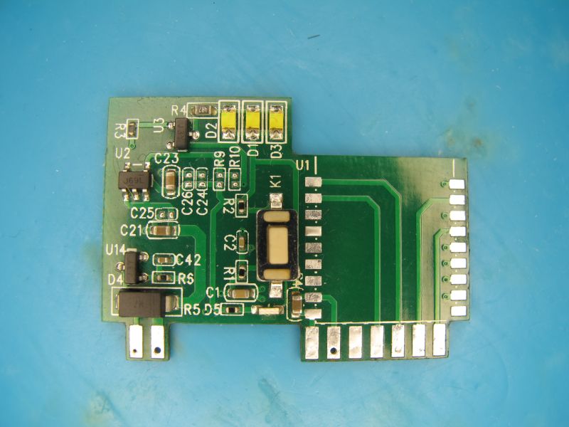
WiFiBoard V1.6:
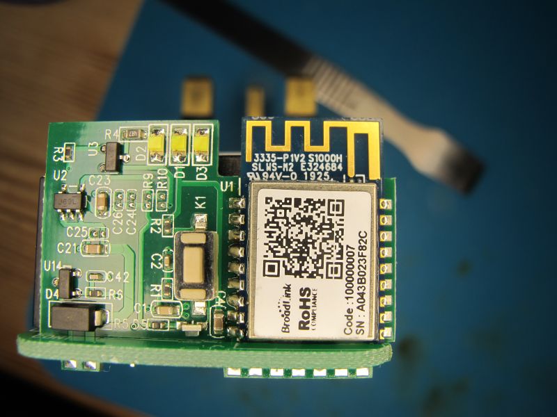
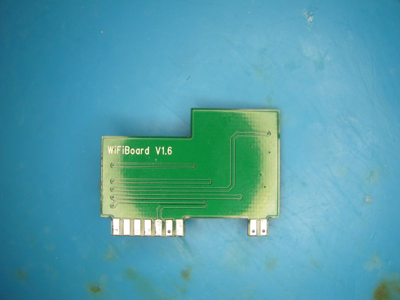
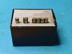
With BL3335-P module de-soldered with hot air gun
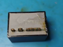
BL3335-P without RF shield reveals BroadLink have labelled this as BL0908. It can be seen in FCC documents marked as RDA5981A
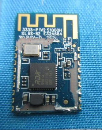
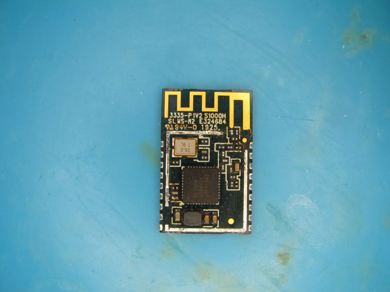
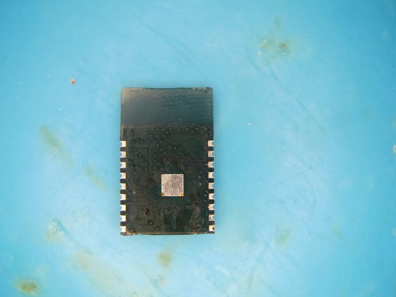
The 3335-P1V2 S1000H SLWS-M2 E324684 module appears to be a BroadLink creation based on the 1mb RDAMicro RDA5981A MCU. The FCC pages supply a datasheet for this module which I attach here.
Overview:
The BL3335-P is a low-cost embedded Wi-Fi module developed by BroadLink for smart home, IoT, and industrial applications. It integrates a 160 MHz ARM Cortex-M4 processor, Wi-Fi transceiver, MAC, baseband, and full TCP/IP stack.
Key Features
Supports IEEE 802.11 b/g/n (20 MHz and 40 MHz bandwidth)
Encryption: WEP, WPA, WPA2 (TKIP/AES)
Wi-Fi modes: STA, AP, and STA + AP
SmartConfig and AP configuration supported
TLS/SSL protocols supported
PCB antenna integrated (no external antenna option)
TCP/IP stack: IPv4, TCP/UDP/FTP/HTTP/HTTPS/TLS/mDNS
Interfaces:
2 × UART
1 × SPI
1 × I²C
4 × PWM
Up to 14 GPIOs
1 × 10-bit ADC (0–2 V input range)
Power supply: 3.3 V (must not drop below 3.3 V)
Operating temperature: –10 °C to +85 °C
Form factor: Stamp-style SMD package
Pad Definitions
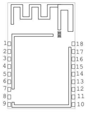
RDA5981 is a 2.4 GHz Wi-Fi SoC family with an ARM Cortex-M4 (up to 160 MHz) and an integrated 802.11b/g/n MAC/PHY/RF (PA/LNA on-chip). It supports STA/softAP/P2P, WPA/WPA2/WEP (TKIP/CCMP), and ships in a tiny 5×5 mm QFN-40. Typical I/O: 2×UART, 2×I2S, I²C, 4×SPI, SDMMC, USB 2.0 (Device/Host), 8×PWM, 2-ch ADC, plus TRNG and AES/RSA accelerators. Firmware stacks seen in docs (all attached) include FreeRTOS and mbed OS.
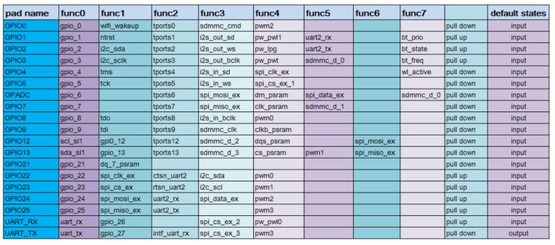
GPIO configuration function summary table
Application Circuit
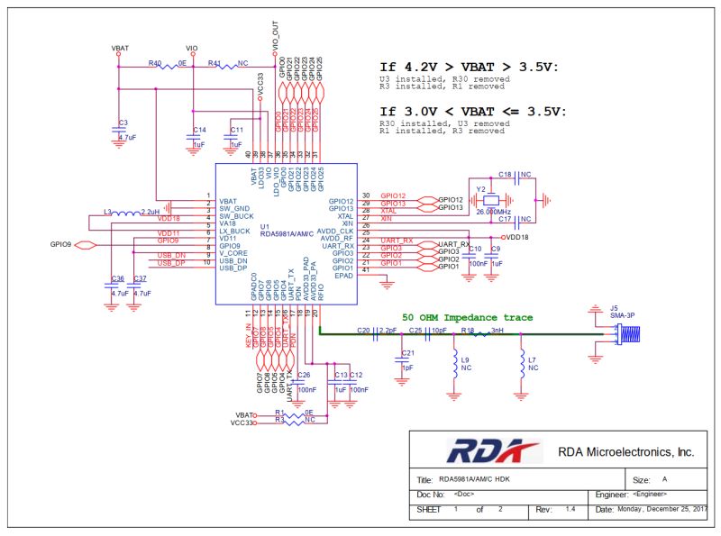
RDA5981 can be seen at the heart of other modules, besides the BroadLink, such as the Hi-Link HLK-M50 and Tuya WRD2L, TYWRD2S and TYWRD3S. More Tuya info here: https://www.elektroda.com/rtvforum/topic4105474.html#21634746
RDA5981A / B / C – Core Features
--------------------------------
• CPU: ARM Cortex-M4 @ up to 160 MHz (with FPU)
• Flash: 8 Mbit (A), 16 Mbit (B), 32 Mbit (C) in-package SPI-NOR
• SRAM: 352–448 KB total (128 KB user A/B, 192 KB user C)
• Wi-Fi: 2.4 GHz 802.11 b/g/n (HT20/HT40 up to 150 Mbps)
• Security: AES / RSA hardware engine, TRNG, secure boot support
• Interfaces:
- 2 × UART
- 1 × I²C
- 4 × SPI (master/slave capable)
- 2 × I²S (audio)
- 1 × USB 2.0 (Device/Host)
- 1 × SDIO / SDMMC
- 8 × PWM
- 2 × ADC (10-bit GPADC0 / GPADC1)
- Up to ~24 GPIO (package-limited)
• Package: QFN-40 (5 × 5 mm, 0.4 mm pitch)
• Supply voltage: 2.7 V – 3.6 V
• Operating temperature: –40 °C to +85 °C
• Crystal: 26 MHz (±10 ppm typical)
Back to the SP4L-UK.
The riser contacts trace to these functions from the module
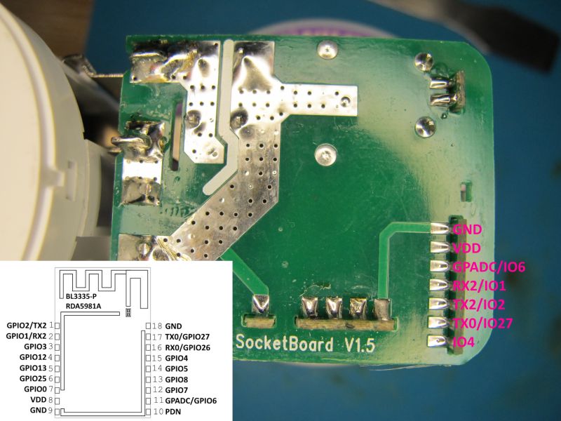
Which means that for debug log capture and flashing purposes we'll need to connect directly to RX0/IO26 on the module because only TX0/IO27 is routed out.
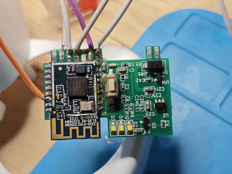
Unfortunately debug log at any baud appears to be obfuscated/protected, requiring GPIO21 to be pulled high to unscramble. This is awkward on the BL3335-P because IO21 is not routed out. The careful placement of 3.3v through a needle point was required.
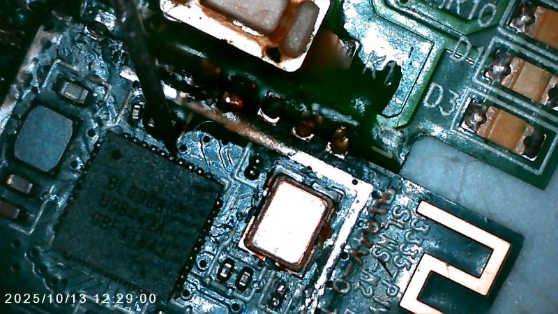
The needle can be released after power-up. At 921600 baud:
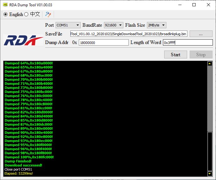
To backup the 1mb flash, the RDA Dump Tool available from within SingleDownloadTool_V01.00.12_20201023.zip at https://github.com/openshwprojects/FlashTools/tree/main/RDAMicro is to be used.
dump start address should be 18000000 (or 18001000 to exclude bootloader) with length of word 0x3fc00
If you set length of 0x3ffff (with flash size 1mb selected in drop-down) the tool will error with

but then 0x3fc00 creates a file that's 1,044,480 bytes which is 4,096 bytes short of the full 1mb. For this reason I chose 0x7fc00 as the length which is just short of 2mb. The file can be trimmed down in HxD later. Alternatively, select 2mb flash size and word length of 0x3ffff. For RDA5981 variants that include 2/4mb flash, adjust word length accordingly.
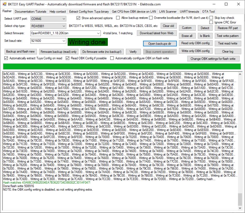
With the factory firmware backup* out of the way, the latest OpenRDA5981 from the releases page can be written to replace the stock firmware.
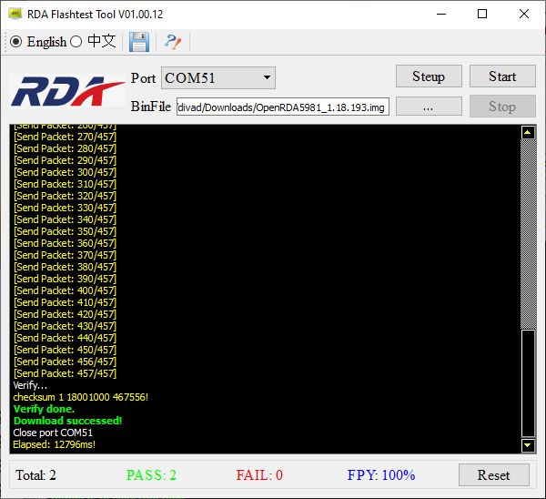
In the RDA Flashtest Tool (change file filter to *.img to show firmware file to choose (release binary may change back to .bin so this may not be required)) OpenRDA5981 should be written to destination address 0x1000
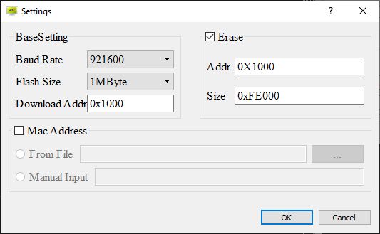
The tool will not allow start address to be below 0x1000.
On this BroadLink device IO21 needed to be held high for flashing to begin, like it does to reveal legible debug log. Again, IO21 doesn't need to be held high, just high at power-on.
It should be noted that this may not always be the case. @gandi69's BG Electrical device with the same module did not require any IO21 action: https://www.elektroda.com/rtvforum/topic4105474.html#21716496
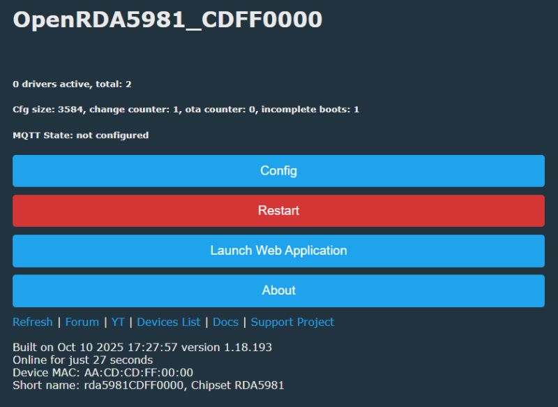
After a power-cycle OpenRDA5981 can be seen booting, displaying plain-text boot log from TX0 (bootloader text remains obfuscated unless IO21 high), and broadcasting starter AP to which connected devices can browse to 192.168.4.1 to get started with OpenRDA configuration.
OpenRDA boot log
In the next post I will configure the pins required to get working relay/button/LED and MQTT for Home Assistant.
For the history of OpenRDA5981 development, including tests with an HLK-M50, see this thread: https://www.elektroda.com/rtvforum/topic4105474.html
*backup can be flashed back in the same way as flashing OpenRDA. If backup was taken from 18000000 then trim away the first 0x1000 or the flasher will complain about oversized image

Opening begins with the removal of the 3 triangle-head screws on the underside. These hold the main case together and the plug cover plate in place.


I removed the plate around power pins and used a spudger to prize open the case. Note the position of the clips. It's quite easy to break those with too much force in the wrong locations.


Inside we see the BroadLink 100-240VAC -> 5V DC power module alongside a Hongfa HF115F 005-1HS3 miniature electromechanical high power relay with a contact rating of 16 A at 250 VAC.

On the other side is found the mains AC and Ground planes, a silkscreen label of "SocketBoard V1.5" and the soldered contacts of the riser which holds the BL3335-P module.
WiFiBoard V1.6:


With BL3335-P module de-soldered with hot air gun

BL3335-P without RF shield reveals BroadLink have labelled this as BL0908. It can be seen in FCC documents marked as RDA5981A


The 3335-P1V2 S1000H SLWS-M2 E324684 module appears to be a BroadLink creation based on the 1mb RDAMicro RDA5981A MCU. The FCC pages supply a datasheet for this module which I attach here.
Overview:
The BL3335-P is a low-cost embedded Wi-Fi module developed by BroadLink for smart home, IoT, and industrial applications. It integrates a 160 MHz ARM Cortex-M4 processor, Wi-Fi transceiver, MAC, baseband, and full TCP/IP stack.
Key Features
Supports IEEE 802.11 b/g/n (20 MHz and 40 MHz bandwidth)
Encryption: WEP, WPA, WPA2 (TKIP/AES)
Wi-Fi modes: STA, AP, and STA + AP
SmartConfig and AP configuration supported
TLS/SSL protocols supported
PCB antenna integrated (no external antenna option)
TCP/IP stack: IPv4, TCP/UDP/FTP/HTTP/HTTPS/TLS/mDNS
Interfaces:
2 × UART
1 × SPI
1 × I²C
4 × PWM
Up to 14 GPIOs
1 × 10-bit ADC (0–2 V input range)
Power supply: 3.3 V (must not drop below 3.3 V)
Operating temperature: –10 °C to +85 °C
Form factor: Stamp-style SMD package
Pad Definitions

| pin | Function 1 | Function 2 | Function 3 | Function 4 | Function 5 | Default state | 1 | GPIO2 | TX2 | UP | 2 | GPIO1 | RX2 | I2C_SDA | UP | 3 | GPIO3 | I2C_SCK | UP | 4 | GPIO12 | SPI_MOSI | DOWN | 5 | GPIO13 | SPI_MISO | PWM1 | DOWN | 6 | GPIO25 | PWM3 | DOWN | 7 | GPIO0 | PWM2 | DOWN | 8 | VDD | 9 | GND | 10 | PDN | 11 | GPADC | GPIO6 | DOWN | 12 | GPIO7 | DOWN | 13 | GPIO8 | PWM0 | DOWN | 14 | GPIO5 | SPI_CS | DOWN | 15 | GPIO4 | SPI_CLK | DOWN | 16 | RX0 | GPIO_26 | DOWN | 17 | TX0 | GPIO_27 | DOWN | 18 | GND |
RDA5981 is a 2.4 GHz Wi-Fi SoC family with an ARM Cortex-M4 (up to 160 MHz) and an integrated 802.11b/g/n MAC/PHY/RF (PA/LNA on-chip). It supports STA/softAP/P2P, WPA/WPA2/WEP (TKIP/CCMP), and ships in a tiny 5×5 mm QFN-40. Typical I/O: 2×UART, 2×I2S, I²C, 4×SPI, SDMMC, USB 2.0 (Device/Host), 8×PWM, 2-ch ADC, plus TRNG and AES/RSA accelerators. Firmware stacks seen in docs (all attached) include FreeRTOS and mbed OS.
| Variant | Flash size (Mbit, in-package) | Max CPU frequency (MHz) | Internal SRAM (KB, total) | User-accessible SRAM | Wi-Fi standard | Package | Voltage range (V) | RDA5981A | 8 | 160 | 352–448 | 128 | 802.11b/g/n | QFN40 5x5mm | 2.7–3.6 | RDA5981B | 16 | 160 | 352–448 | 128 | 802.11b/g/n | QFN40 5x5mm | 2.7–3.6 | RDA5981C | 32 | 160 | 352–448 | 192 | 802.11b/g/n | QFN40 5x5mm | 2.7–3.6 |
GPIO configuration function summary table

Application Circuit

RDA5981 can be seen at the heart of other modules, besides the BroadLink, such as the Hi-Link HLK-M50 and Tuya WRD2L, TYWRD2S and TYWRD3S. More Tuya info here: https://www.elektroda.com/rtvforum/topic4105474.html#21634746
RDA5981A / B / C – Core Features
--------------------------------
• CPU: ARM Cortex-M4 @ up to 160 MHz (with FPU)
• Flash: 8 Mbit (A), 16 Mbit (B), 32 Mbit (C) in-package SPI-NOR
• SRAM: 352–448 KB total (128 KB user A/B, 192 KB user C)
• Wi-Fi: 2.4 GHz 802.11 b/g/n (HT20/HT40 up to 150 Mbps)
• Security: AES / RSA hardware engine, TRNG, secure boot support
• Interfaces:
- 2 × UART
- 1 × I²C
- 4 × SPI (master/slave capable)
- 2 × I²S (audio)
- 1 × USB 2.0 (Device/Host)
- 1 × SDIO / SDMMC
- 8 × PWM
- 2 × ADC (10-bit GPADC0 / GPADC1)
- Up to ~24 GPIO (package-limited)
• Package: QFN-40 (5 × 5 mm, 0.4 mm pitch)
• Supply voltage: 2.7 V – 3.6 V
• Operating temperature: –40 °C to +85 °C
• Crystal: 26 MHz (±10 ppm typical)
Back to the SP4L-UK.
The riser contacts trace to these functions from the module

Which means that for debug log capture and flashing purposes we'll need to connect directly to RX0/IO26 on the module because only TX0/IO27 is routed out.
Quote:In default, UART2 (pin1 and pin2) are used for bypass communication and UART0 (pin16 and pin17) are used for output of debugging information and burning firmware.

Unfortunately debug log at any baud appears to be obfuscated/protected, requiring GPIO21 to be pulled high to unscramble. This is awkward on the BL3335-P because IO21 is not routed out. The careful placement of 3.3v through a needle point was required.

The needle can be released after power-up. At 921600 baud:
Code: Text
To backup the 1mb flash, the RDA Dump Tool available from within SingleDownloadTool_V01.00.12_20201023.zip at https://github.com/openshwprojects/FlashTools/tree/main/RDAMicro is to be used.
dump start address should be 18000000 (or 18001000 to exclude bootloader) with length of word 0x3fc00
If you set length of 0x3ffff (with flash size 1mb selected in drop-down) the tool will error with

but then 0x3fc00 creates a file that's 1,044,480 bytes which is 4,096 bytes short of the full 1mb. For this reason I chose 0x7fc00 as the length which is just short of 2mb. The file can be trimmed down in HxD later. Alternatively, select 2mb flash size and word length of 0x3ffff. For RDA5981 variants that include 2/4mb flash, adjust word length accordingly.

With the factory firmware backup* out of the way, the latest OpenRDA5981 from the releases page can be written to replace the stock firmware.
In the RDA Flashtest Tool (change file filter to *.img to show firmware file to choose (release binary may change back to .bin so this may not be required)) OpenRDA5981 should be written to destination address 0x1000

The tool will not allow start address to be below 0x1000.
On this BroadLink device IO21 needed to be held high for flashing to begin, like it does to reveal legible debug log. Again, IO21 doesn't need to be held high, just high at power-on.

It should be noted that this may not always be the case. @gandi69's BG Electrical device with the same module did not require any IO21 action: https://www.elektroda.com/rtvforum/topic4105474.html#21716496
After a power-cycle OpenRDA5981 can be seen booting, displaying plain-text boot log from TX0 (bootloader text remains obfuscated unless IO21 high), and broadcasting starter AP to which connected devices can browse to 192.168.4.1 to get started with OpenRDA configuration.

OpenRDA boot log
Code: Text
In the next post I will configure the pins required to get working relay/button/LED and MQTT for Home Assistant.
For the history of OpenRDA5981 development, including tests with an HLK-M50, see this thread: https://www.elektroda.com/rtvforum/topic4105474.html
*backup can be flashed back in the same way as flashing OpenRDA. If backup was taken from 18000000 then trim away the first 0x1000 or the flasher will complain about oversized image


