






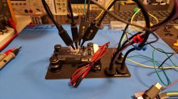

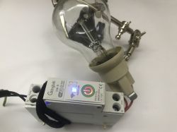
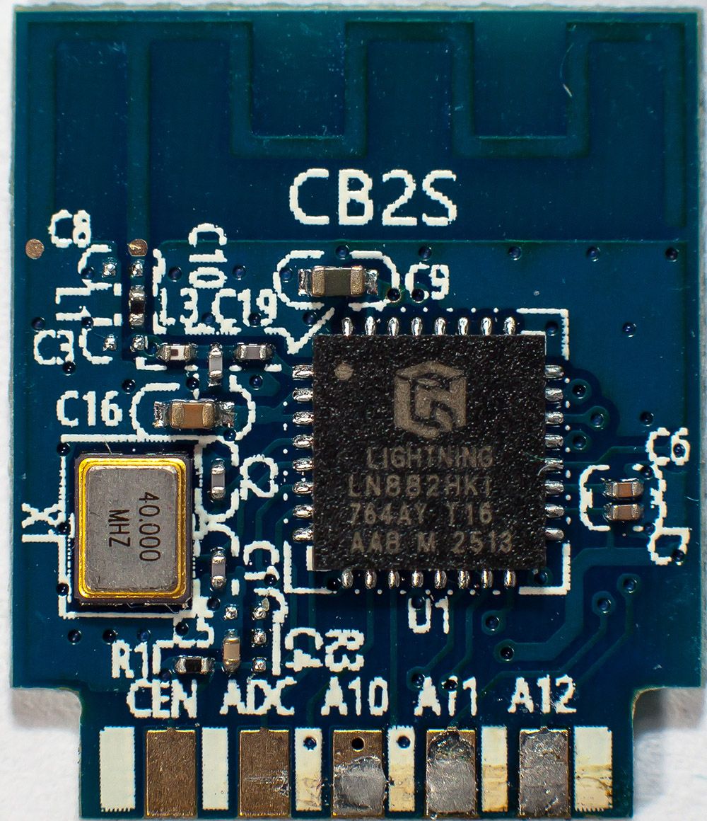
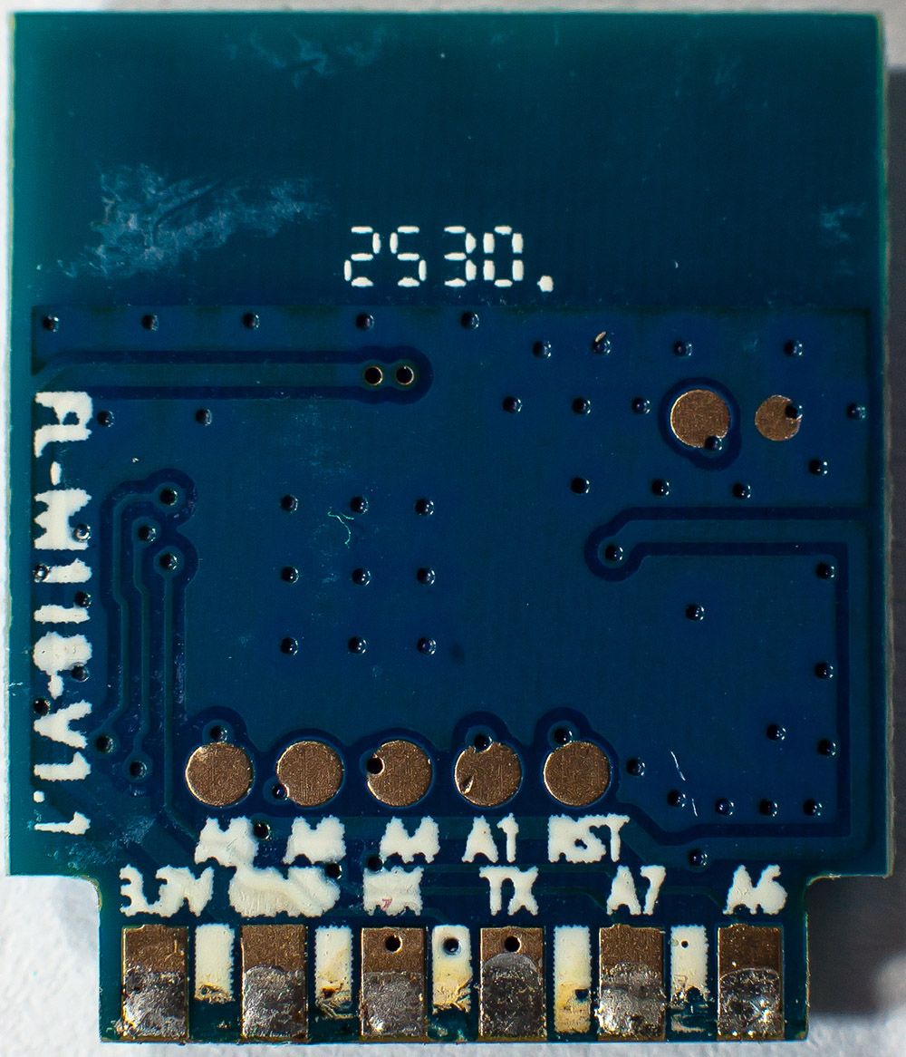
I am here after buying an UPXNBOR plug expecting to get another esp device for Tasmota. After teardown - which is fortunately still very easy with those plugs - I learned that it has no longer an Esp chip in, but an LN882HKI. I desoldered the chip, as the prints on the pins are very ugly and almost not to read, while it is soldered in. But even when I have this chip in front of me, the prints are very bad.
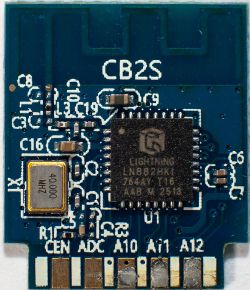
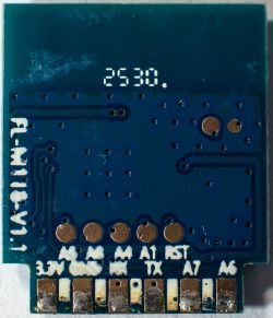
I learned now that OpenBeken would be the way to go, as this should work similar to my Tasmota devices.
First question here:
Where do I have to solder which pins from my 3.3 V USB-TTL adapter?
Which pin can I use for connecting a buzzer to?
Thanks for any useful hints on how I can proceed without damaging the µC.
Edit:
When watching now my pictures I have shot for this post, another question arised:
Why are C3, C4, C5 and C8 not placed and contain empty solder pads?
More questions arise:
Is the 3V3 50mA output from an FT232 adapter enough to power such an desoldered chip? Or does the µC needs higher current?
Added after 5 [hours] 31 [minutes]:
Ok, did some more research, found the datasheet and looked closer to the device. I marked some traces and vias and created an transparent mirrored overlay of the backside, to get an better overview, what is routed where.
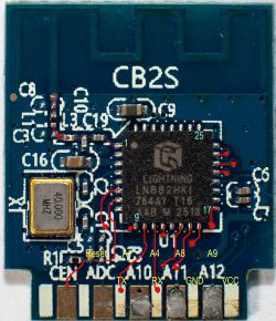
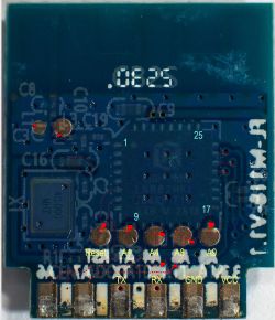
I was shocked reading in the datasheet, that there are up to three UARTs, but they have no hard defined pin, pins could be mapped to each IO-pin. However, I found some articles, telling me, that initially TX maps to A2, which is Pin10, RX maps to A3, which is Pin11. As the mapping for the readable TX with Pin10 is correct, I labeled the neighbour-pin connected to pin 11 RX
So still waiting for some responses before I fry the µC, by wronmg assumptions.
I learned now that OpenBeken would be the way to go, as this should work similar to my Tasmota devices.
First question here:
Where do I have to solder which pins from my 3.3 V USB-TTL adapter?
Which pin can I use for connecting a buzzer to?
Thanks for any useful hints on how I can proceed without damaging the µC.
Edit:
When watching now my pictures I have shot for this post, another question arised:
Why are C3, C4, C5 and C8 not placed and contain empty solder pads?
More questions arise:
Is the 3V3 50mA output from an FT232 adapter enough to power such an desoldered chip? Or does the µC needs higher current?
Added after 5 [hours] 31 [minutes]:
Ok, did some more research, found the datasheet and looked closer to the device. I marked some traces and vias and created an transparent mirrored overlay of the backside, to get an better overview, what is routed where.
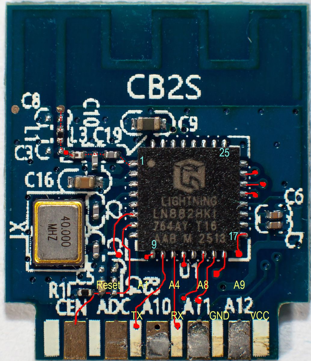
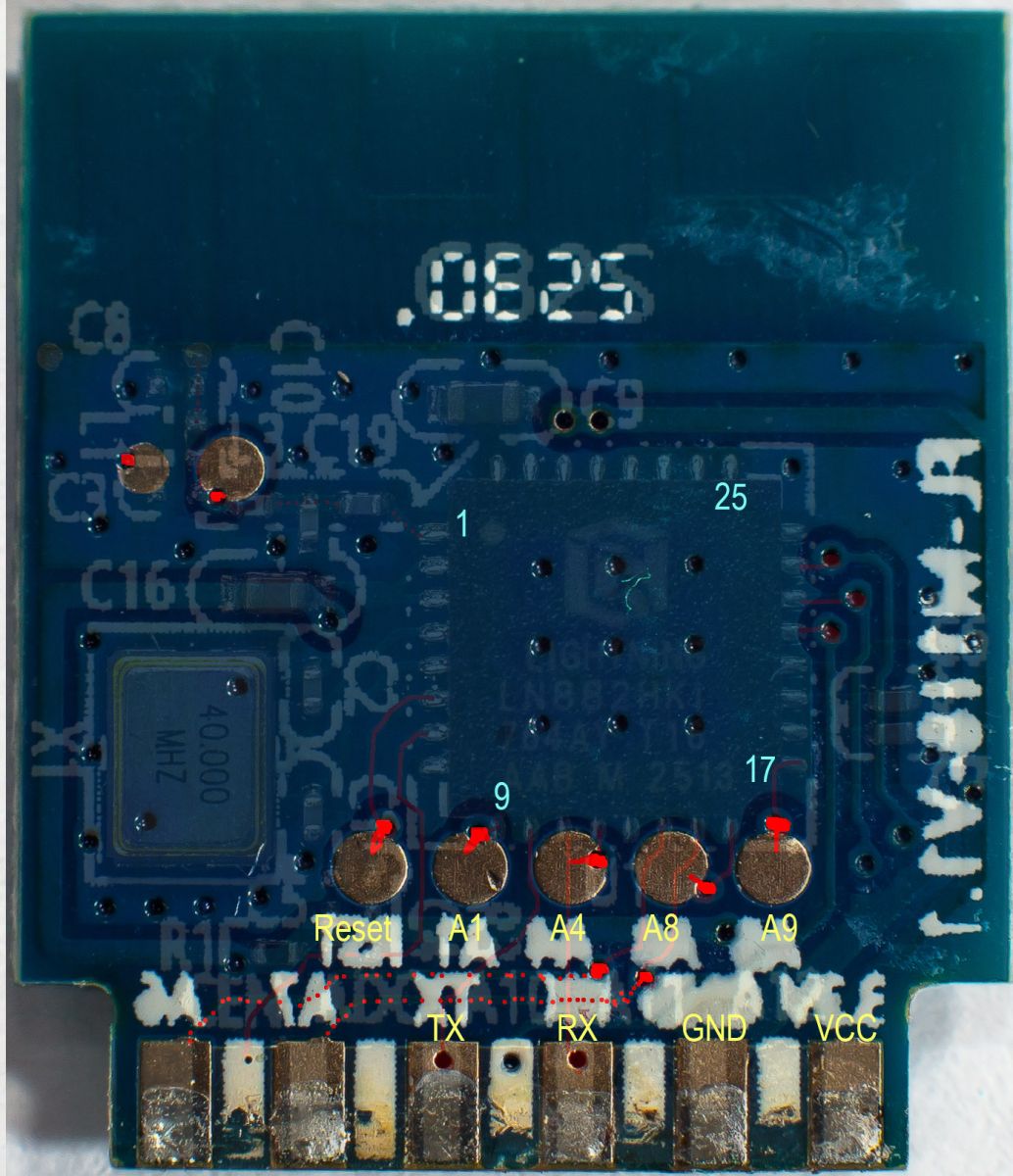
I was shocked reading in the datasheet, that there are up to three UARTs, but they have no hard defined pin, pins could be mapped to each IO-pin. However, I found some articles, telling me, that initially TX maps to A2, which is Pin10, RX maps to A3, which is Pin11. As the mapping for the readable TX with Pin10 is correct, I labeled the neighbour-pin connected to pin 11 RX
So still waiting for some responses before I fry the µC, by wronmg assumptions.
