logo elektroda
logo elektroda
X
logo elektroda

Taobao Tuya BK7252UQN68 Bare A9 Cam PCB (SC-10024 v1.0.0) - UART/SPI Flash Backup - OpenBK7252

divadiow 4017 76
ADVERTISEMENT
  • #61 21706892
    insmod
    Level 31  
    >>21706885
    Yes, and it's that way on every beken, whether encrypted or not.
    Every 32 bytes of data is followed by 2 bytes of crc

    You can create a script that would remove those bytes to get readable strings, if required.
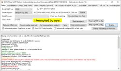
  • ADVERTISEMENT
  • Helpful post
    #62 21706923
    p.kaczmarek2
    Moderator Smart Home
    That's a ... a very common occurence of CRC, isn't it? I was under impression that mere bits are needed to check the validity of very large buffers, and here they use 16 bits per 32 bytes...

    I think I can read, erase and write memory now - also with full chip erase (and with status register checks):
    Terminal window showing flash memory read/write via SPI interface
    Nothing really new here, the same I did there: https://github.com/openshwprojects/OpenBK7231T_App/blob/main/src/driver/drv_spi_flash.c
    I will pack this into some C# class and prepare either a standalone tool or a EF update.. or both, not sure.

    Added after 16 [minutes]:

    I ordered one camera from local supplies, but I have a feeling it will be XR again.
    Mini Wi-Fi camera with smartphone app showing live footage
    Helpful post? Buy me a coffee.
  • ADVERTISEMENT
  • #64 21707462
    p.kaczmarek2
    Moderator Smart Home
    @divadiow this Beken SPI is basically generic SPI + Beken RESET. As you probably know... since you've used NeoProgrammer.
    This brings the question - can we use EF as generic SPI flasher? I think we can! Do you have BIOS chips to try?

    My next camera is with delivery courier.
    Helpful post? Buy me a coffee.
  • ADVERTISEMENT
  • #65 21707472
    divadiow
    Level 38  
    p.kaczmarek2 wrote:
    Do you have BIOS chips to try?


    Taobao Tuya BK7252UQN68 Bare A9 Cam PCB (SC-10024 v1.0.0) - UART/SPI Flash Backup - OpenBK7252
    plus all the usual loose chips and actual devices...
  • #66 21707477
    p.kaczmarek2
    Moderator Smart Home
    What kind of board is it? I haven't seen it yet. I only do this that way:
    https://www.elektroda.pl/rtvforum/topic3993012.html
    Helpful post? Buy me a coffee.
  • ADVERTISEMENT
  • #68 21707518
    p.kaczmarek2
    Moderator Smart Home
    Ok I think I've found them. I was not aware that there is this kind of breakout, but it makes sense in a hindsight.
    W25Q32 flash memory module with SPI interface on blue PCB board
    Helpful post? Buy me a coffee.
  • #69 21707521
    divadiow
    Level 38  
    ok, sure. yes. Ali Express, the cave of wonders
  • #70 21738867
    divadiow
    Level 38  
    >>21705726

    still curious about this. did you pursue anything else with it?

    I want to play more but time (and speed/skill level) is, as always, the limiter.

    I started to look at XF16 JPEG build but lost momentum for now.

    The Xradio documentation looks quite good for SDK/Jpeg dev
  • #71 21761349
    divadiow
    Level 38  
    insmod wrote:
    https://github.com/NonPIayerCharacter/OpenBK7231T_App/actions/runs/18136281276 if interested
    BK7252N and BK7252 log is on UART1


    Code: Text
    Log in, to see the code


    thought I'd give this a go. not found where IOs set are used yet though in cam build.

    This is a new 18-pin cam doorbell BK7252UQN48, not Tuya, unencr.

    J1 camera module pinout diagram with DVP signal labels and P0–P39 mappings
  • #72 21773315
    easton
    Level 1  
    >>21706031
    Based on the boot logs (SDK 3.0.33), the BK7252UQN48 appears to be the older BK7252 core (BLE 4.2), not the newer BK7252N (BLE 5.2). It looks like 'U' just denotes the QFN48 package for the original silicon.

    This naming matches the pattern seen in the BK72XX_SDK_User_Manual-3.0.3.pdf (attached) for the BK7231, where 'U' was the older BLE 4.2 core and 'N' was the upgrade to BLE 5.1.

    The pin mapping for BK7252UQN48 matches the BK7252N datasheet QFN48 (attached), so you can use that to trace the UART pins.
    Attachments:
    • BK7252N 数据手册_V1.13_en.pdf (3.47 MB) You must be logged in to download this attachment.
    • BK7252_Data_Sheet_Chip_Specification_V1.3.pdf (682.14 KB) You must be logged in to download this attachment.
    • BK72XX_SDK_User_Manual-3.0.3.pdf (705.04 KB) You must be logged in to download this attachment.
  • Helpful post
    #73 21773580
    divadiow
    Level 38  
    well, regarding a QFN48 U and N pin comparison, here is my independent work-in-progress tracing of IOs on BK7252UQN48 alongside the BK7252N QFN48 from the datasheet. I'd not married the two until now.

    Pin mapping comparison of BK7252N and BK7252UQN48 in QFN48 package

    not sure what to make of the GNDDIG label now though. I'm sure it had continuity with GND. I'll recheck.


    EDIT: Updated image correcting GNDDIG label for VDDRAM
  • #74 21773619
    p.kaczmarek2
    Moderator Smart Home
    Helpful post? Buy me a coffee.
  • #75 21773623
    divadiow
    Level 38  
    Well that was my assumption based on BK7252U QFN68 label, which is known, and the fact that it had continuity with ground. The thing now is that, if it is indeed GNDDIG, then that differs from the BK7252N datasheet, and so the BK7252N pin diagram can't be totally relied on for understanding BK7252U QFN48. I hope that makes sense!
  • #76 21773630
    p.kaczmarek2
    Moderator Smart Home
    Well, putting VDD in place of GND is a serious change. Even the PIC microcontrollers, which I used to program during school days, try to keep their VDD/GND footprint compatible between MCU variations. And here we have a straight up power to ground swap...
    EDIT: IMAGE REMOVED TO AVOID CONFUSION
    Helpful post? Buy me a coffee.
  • #77 21773645
    divadiow
    Level 38  
    Yep ok. Will confirm with continuity and voltage measurement later today

    Added after 7 [hours] 7 [minutes]:

    yikes. it carries a voltage. 3.62v. original image updated. annoying because I usually triple-check to avoid exactly this.

Topic summary

✨ A bare A9-type PCB (SC-10024 v1.0.0) featuring the BK7252UQN68 chip was purchased from Taobao without camera, battery, or casing. The board includes an 18-pin camera connector, two buttons, and two LEDs (red and two-tone blue/green). Attempts to obtain an SDK from the seller were unsuccessful. Efforts to locate Tuya firmware download URLs programmatically also failed. Flashing combined OpenBK7252 firmware files enabled OTA functionality on first boot, confirming OTA support despite requiring SPI flash programming. Logs indicate successful OTA initialization and app partition erase/write operations. Some malloc failures were observed, possibly due to differences in memory allocation methods between OTA and default A9 bootloader environments. Further testing or suggestions for additional experiments were requested.
Generated by the language model.

FAQ

TL;DR: OTA wrote 794,045 bytes on first boot; "we see OTA process on first boot". Flash OBK by merging bin+rbl, map pads to CH341A, and back up the 4 MB flash. For hardware hackers needing flash backups, OTA layout, and Tuya pairing notes. [Elektroda, divadiow, post #21570898]

Why it matters: It shows how to safely dump, flash, and OTA‑upgrade BK7252 A9 camera PCBs without bricking, using low‑cost tools.

Quick Facts

What is this Taobao BK7252 A9 camera PCB and its hardware layout?

It’s a bare A9-style camera PCB marked SC-10024 v1.0.0 using a BK7252UQN68. It includes an 18‑pin camera connector, two buttons, and two LEDs (one red and one blue/green two‑tone). No camera module, battery, or case ship with it. [Elektroda, divadiow, post #21557995]

How do I wire the test pads to a CH341A to back up the SPI flash?

Pad map: CE/CEN→D2, SCK→SCK, CSN→CS0, SI→MOSI, SO→MISO, GND→GND. Then use Beken SPI mode with a CH341A and NeoProgrammer. How‑To: 1) Solder flying leads to pads. 2) Enter Beken SPI mode and power the board. 3) Detect XTX XT25F32B and dump the 4 MB image. [Elektroda, divadiow, post #21557995]

What flash chip and capacity does it use?

The board carries an XTX XT25F32B SPI NOR. Capacity is 32 Mbit (4 MB). Reported SPI ID is 0x0B4016. NeoProgrammer recognizes it reliably for dumps. [Elektroda, divadiow, post #21557995]

What UART settings should I use and what indicates a healthy boot?

Use 115200 baud on TX1. A healthy boot shows BK7251_x logs, Tuya initialization, BLE advertising, and AP start as SmartLife‑2640. You’ll also see Wi‑Fi and watchdog initialization entries and LED status changes in logs. [Elektroda, divadiow, post #21557995]

How can I flash OpenBK7252 and trigger the OTA upgrade on first boot?

Merge OpenBK7252_QIO7231u_t_c1b0ac146bf0.bin with OpenBK72527231u_t_c1b0ac146bf0.rbl at 0x132000 and flash from 0x0. On first boot, the OTA engine writes 794,045 bytes to the app partition, then boots OBK. Watch serial logs to confirm erase and write progress. [Elektroda, divadiow, post #21570898]

Does OTA work on this A9 BK7252 board?

Yes. “So, OTA works.” Users report success, though initial SPI flashing may be needed to stage images. Using the default A9 bootloader helped in testing. [Elektroda, insmod, post #21570913]

Why do OTA uploads via the web GUI fail with “malloc failed”?

Logs show OTA attempts via the web and GUI ending with “malloc failed.” A practical workaround is pre‑staging the RBL at 0x132000 and flashing a merged image so the device upgrades itself on first boot. [Elektroda, divadiow, post #21570898]

What OTA layout and addresses are involved on this board?

The boot log shows a ping‑pong scheme erasing the download RBL at 0x132000. Combining the .bin base and .rbl at that offset enabled the on‑boot OTA to rewrite the app partition. [Elektroda, divadiow, post #21570898]

How far can the built‑in UART preset read, and how do I dump the full 4 MB?

The standard BK7252 preset read stops around 2 MB. Use the EF custom read from 0x11000 via TX2/RX2 to reach the end, or use CH341A SPI to dump the full 4 MB directly. [Elektroda, divadiow, post #21557995]

Which OpenBK builds boot correctly on this board?

OpenBK7252_QIO7231u_t_c1b0ac146bf0.bin boots into OBK. The OpenBK7252_Tuya_QIO7231u_t_c1b0ac146bf0.bin shows bootloader output but no app, ending with an ARM anomaly on jump. [Elektroda, divadiow, post #21557995]

Can I pair it with Tuya and view its data model (DPs)?

Yes. It pairs and reports device details (firmware 1.0.4). The model exposes DPs such as basic_indicator, basic_nightvision, sd_status, sd_format, record_switch, device_restart, and others useful for IPC features. [Elektroda, divadiow, post #21557995]

Is an SDK available for this board or Tuya IPC?

The seller did not provide the SDK. However, public TuyaOS IPC demo archives exist (tuyaos_demo_ipc versions 1.0.x through 1.1.50) hosted on Tuya’s Airtake storage. [Elektroda, divadiow, post #21570227]

How do I enter Beken SPI mode and verify flash access?

After wiring the pads, power the board and use the Beken SPI Python tool with CH341A. NeoProgrammer should detect XTX XT25F32B (ID 0x0B4016) and allow read/write operations, confirming SPI access. [Elektroda, divadiow, post #21557995]

What LEDs and buttons exist, and can I control indicators from Tuya?

The PCB has two buttons and two LEDs: a single red and a blue/green bi‑color. The Tuya DP basic_indicator toggles the status LED behavior from the app’s settings page when paired. [Elektroda, divadiow, post #21557995]

Should I remove series resistors when repurposing lines as GPIOs?

Yes. Remove the series resistors to avoid unintended loading and get clean GPIO behavior. As an expert noted, “it’s better to remove those resistors.” [Elektroda, p.kaczmarek2, post #21617875]
Generated by the language model.
ADVERTISEMENT