I decided to write this guide, because you can't find anything about it on the net (or I'm not doing a good job searching).
There is a lot about some bizarre indirect methods using software that you don't know where to get. And this method is simple and effective.
The guide is the end result of a whole pile of wasted tiles, but I do not regret it, I will reflect on chemicals

To the point
1. Download the pcb-gcode.ulp plugin from the Artsoft website (or from the attachment).
http://www.cadsoftusa.com/downloads/ulps?language=en Works with Eagle version 5 and 6.
2. Unpack and copy to Eagle / ulp directory
3. Run Eagle, on Vista and 7 systems run as administrator.
4. Not a word about design, I assume that we already have the board design ready - open it.
5. Remove unnecessary layers from the PCB designed in the Eagle program, leave only the bottom, pads and vias (the guides will probably be useful).
Of course, I assume that we mill the bottom side.
6. Press file and select the run command - the window with ulp plugs will open (you can press the ULP icon on the main bar).
7. Now select pcb-gcode-setup.ulp - this will allow us to set the milling parameters.
8. In the Machine tab, set the units to millimeters, and go to the Generation Options tab.
9. In the first Generation Options window, select the page to be milled. In this case we check Generate bottom outlines and Generate bottom drils, and we deselect Generate top outlines and Generate top drils. We also mark Mirror. We introduce parameters
in the board window:
show preview (optional), spot drill holes -0.254, minimum 0.00254 mm; Maximum - 0.01 mm; Step size - 0.127 mm. We do not use commas,
only dots - American system.
10. Machine tab. Z High - the height of the safe transport of the tool can be 5 mm. Z Up - how much the tool will lift when changing position without milling, we give 2 mm. With Down - how deeply it will mill the copper - I set it to -0.17 mm. You can set deeper, but such thin cutters are tapered,
so they will widen the milled area and the board may not come out. We set the drill depth to -1.8 mm (it should be enough, if we had a thicker laminate, we set more). Drill dwell - 0.1 (time to stop the cutter in the hole in seconds). Position X and Y zero. Position Z 10.
11. Mark GCode style tab Mach.
12. Press Accept, and finish setting. We confirm OK and once again Accept. The rest of the parameters remain the default.
13. Find pcb-gcode.ulp and click twice.
14. In a moment, the program will generate two files placed in the same directory as the board project projekt.brd.
These will be files: project.bot.drill.tap and project.bot.etch.tap. These are files already accepted by the Mach program. Preferably instead of dots in the middle
put underscores in the names, because mach sees them right away.
15. Now it would be good to check the board for errors. For this I used the older, free version of CamBam.
Operation very simple, at least when it comes to the preview.
If the honorable commission did not find any errors, we start milling the insert. Do not underestimate this check, especially if the distances between paths in the project are small. Then the adjacent tracks or pads can "merge" with each other. Then you have to correct the design.
16. First, upload the project_bot_etch.tap file and install a 0.2 mm cutter. Where the G-code will start, you have to check it "dry".
Usually it is near the lower left corner.
We will set the cutter to "0" and continue as in Mach - reset all positions and start. The milling machine will replace the litter box with chemicals.
17. When it is finished, pick up the tool so that it can be replaced with a drilling cutter. Then we set it to zero in the X and Y axes (the place where the program started milling).
Reset the Z axis after a tool change. In order not to manually set the zero in the X and Y axes, you can add in the file projekt_bot_etch.tap
(on the second line, the last nodes after the Z position, X00.0000 Y00.0000).
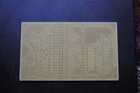
When we have everything set up, upload the file projekt_bot_drill.tap and start. The milling machine will now drill all holes.
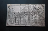
Here is an example of a printed circuit board for Atmega_fusebit_doctor of my friend's manekinen (thanks),
which doctor I'm about to do.
The board is milled with a 0.2 mm cutter, flat face. Holes drilled with a 0.7 mm cutter. If you need to enlarge one of them, I will do it with a tiny hand drill.
No problem if there are pilot holes. After the whole operation, smooth the tile with 1000 sandpaper to get rid of the hail on the edges of the paths.
I took pictures and only realized that I hadn't checked the mirror option, so the board came out wrong - in the mirror. But now that the method is fine-tuned, I'm about to make a new plate. I just don't take a photo, because I gave the camera back. Mobile photos are not suitable for publication. The disadvantage of the method are the fields of unmilled copper remaining between the tracks. For now, I do not know how to get rid of it, maybe I will come up with something, then I will add a sequel.
I just need to buy a laminate
. All the supplies went to the experiments.
In the attachment the CamBam program, which in the free version is already difficult to get. The author has withdrawn it from his site, he only has the paid versions there.
In the second, a plug for Eagle.


Comments
I was just trying to mill the tiles and my friend's article fell out of the sky. It's a great idea to gather this information in one place. [Read more]
And let a colleague write how long it takes to mill an A5 formatted smd board? It's about the profitability of such a game. The preparation of the project takes the same amount and the execution itself... [Read more]
What program are you using to control the machine? [Read more]
Have you figured out the milling of tile contours? I mean some strange shapes and possibly inside a plate for mounting larger elements. Milling in a rectangular insert may be inefficient compared to other... [Read more]
Buddy Kowal011: The time it takes to mill a tile depends on the speed of the machine. At a feed rate of 1300 mm / min, the plate presented in the photo was milling about 10 minutes. Drilling took about... [Read more]
The design may be nice, but diligence is not. The paths are a bit crooked. Why has this happened? Something. A colleague did not try. Even for a PCB made with a marker pen, the layouts fit perfectly.... [Read more]
A great tutorial, and the shape of the paths depends more on the rigidity and accuracy of the machine. I may have a silly question, but how do I open a pcb file in eagle? I have never done it and I just... [Read more]
Thanks for the article. My first test: http://obrazki.elektroda.pl/2971003500_1388697036_thumb.jpg http://obrazki.elektroda.pl/9323286300_1388697044_thumb.jpg http://obrazki.elektroda.pl/2992228200_1388697048_thumb.jpg... [Read more]
Interesting topic, but for me it is rather a curiosity. Perhaps it makes a bit more sense with short bursts. Making precise paths and drilling (without a stand) holes for DIL and SIL housings is not a... [Read more]
And I have one more question: I followed the instructions from the first post and the program generated only the outline of the paths for me, and skipped the subtitles made on the top layer. I wanted to... [Read more]
Generate milling must be selected. Make the outline of the pcb board with a Milling layer [Read more]
I'm having trouble generating the top layer. In the settings, I select generate top outlines / drills, but it still generates only the bottom layer for me. [Read more]
Hello. Is there any Polish description of the CamBam program functions? best regards [Read more]
Hello! He's been doing circuits on a machine I've built for some time. I used to make tiles even on a larger scale using the photo method. I had a digestion unit, the platesetter is still somewhere... [Read more]
Hello, I'm having trouble generating gcode. After performing the activities in accordance with the above instruction, only the * .bot.etch.tap file is generated for me, but the * .bot.drill.tap file... [Read more]
I have never had such a mistake. I'm using version 3.6.2.4 try to install a newer version again because it looks like something is missing. Alternatively, send me the eagle file, I'll check it... [Read more]
Hello, after installing the latest pcb gcode 3.6.2.4 it kicked Java errors. After installing Java, I am also unable to generate the code. I am asking for help in generating the files. The project is... [Read more]
to Luke. I will not tell you anything about mistakes, you definitely have something dug up in your computer. The Eagle staff bow to your project. I recommend some courses that are full of online. I improved... [Read more]
I also had Java bugs, but only when I chose the show preview option. When I checked this, everything is generating nicely. I wanted to check this method when making pcb on aluminum supports. [Read more]