There is such a small, neat and cheap USB Blaster programmer for Altery CPLD / FPGA circuits, which fulfills its role perfectly.
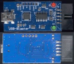
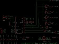
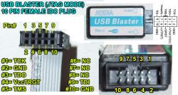
Unfortunately, it does not provide the supply voltage, which requires the programmable circuit to be powered from an external source. Different circuits have different supply voltages (and sometimes even several).
For example, my favorite CPLD EPM3064 has one voltage for supplying the core of the system (VCCINT), and the other for supplying I / O terminal buffers (VCCIO), so that the system can work in a system adapted to different voltages, eg 3.3V, 2.5V.
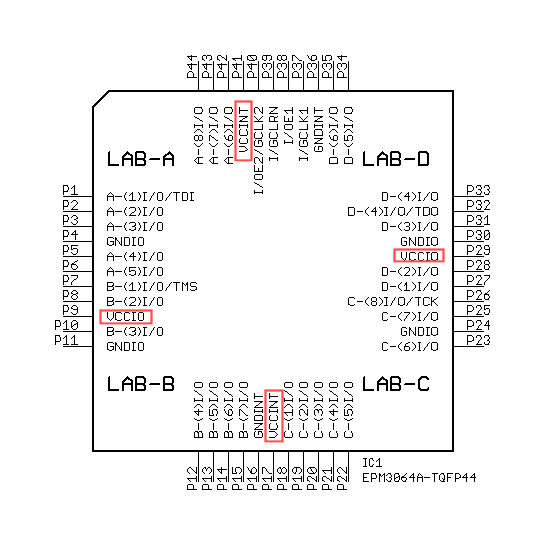
For example, EPM240 has four IOLABS blocks and each of these blocks can have its own VCCIO voltage
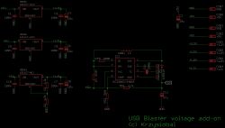
So I came up with the idea of making a small "adapter" for the aforementioned programmer, producing the most popular voltages. The whole thing had to fit into the existing housing, which was quite a challenge. The assumptions were to include the following voltages: + 1.8V, + 2.5V, + 3.3V, + 5V, + 12V.
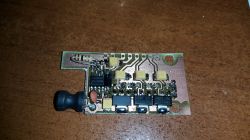
As a result, a board was created, adapted to the size of the existing housing, which is soldered to the programmer's main board with two wires (to ground and + 5V) where the J1 connector is in the original board. The board also has two holes so that LEDs can pass through it, signaling the operation of the original board. We managed to stuff everything on a single-layer PCB, so the PCB can fit tightly to the original one without any fear of a short circuit.
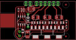

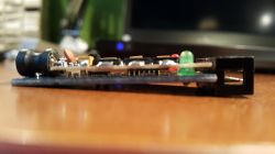
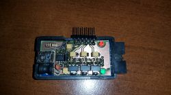
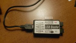
I decided to derive all the tensions using the male goldpin strip, because, unlike the female one, it does not wear out (female strips quickly become loose when inserted frequently). To protect myself against accidental short-circuit of male goldpins at the moment of contact with something, I put a cap on the pins (made of a female goldpin plug)
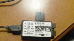
* The + 1.8V, + 2.5V, + 3.3V voltages come from the dedicated AMS1117 stabilizers
* The + 5V voltage comes directly from the USB connector
* I used the MC34063 converter for the + 12V voltage
The reader may ask himself what the presence of + 12V voltage is for? Well, the necessity to have this voltage was basically the reason for the creation of the described PCB. Often, when designing a device, we try to choose a system for it so that it meets the needs, but is not overly "exaggerated" (ie it has the required number of terminals). Too many of the offered and unused pins is not only a waste of price (more expensive system) but also a more complicated PCB (more pins = larger housing = usually more complicated board design)
Therefore, for many needs, e.g. the previously described simple EPM3064 system is sufficient. This circuit has 30 I / O pins. However, I have often been in a situation where I missed that one / two extra pins and had to resort to strange combinations. It turns out that the JTAG programming pins of this system (TDI / TMS / TCK / TDO) can also function as standard I / O pins. In order to force them to do so, in the Quartus environment you should:
1. Right-clicking on a layout, select Device >> Device and Pin Options >> "General" tab
2. Uncheck "Enable JTAG BST Support"
3. Recompile the project
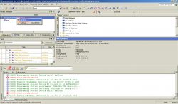
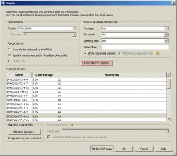
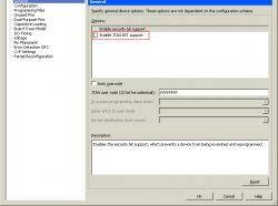
Unfortunately, now trying to select the "POF" file to upload to the system will end up with an enigmatic message "JTAG support distabled in file ..."
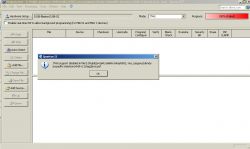
4. So go back to the "Programming files" tab and select "JEDEC STAPL Format File (.jam)" and recompile the project again.
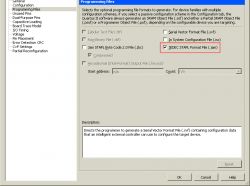
From now on, after each compilation, in addition to the standard POF file, a JAM file will be generated and this file should be selected when programming.
Unfortunately, in order to program (or reprogram) a batch with JTAG pins turned off, you need ... according to the catalog note - a special high-voltage programmer. No wonder, because if now JTAG pins are used as standard I / O pins, how should the system know that we want to reuse them for programming?
However, there is a trick (about which there is not a word in the catalog note) .. If the EPM3064 chip, when turned on, sees + 12V on its I / OE1 pin (in the QFP44 housing it is pin 38), the JTAG pins will become active again (until restart) and they can be used for programming .. Of course, when using this method, you need to keep a few things in mind:
* connect + 12V to the I / OE1 pin for the time of programming MUST with some protection resistor in series (e.g. 1k). I do not know exactly what voltage the system requires, because there is about 8V on the other side of the resistor.
* pin I / OE1 should be either not used at all in the project, or at least secured with a jumper that "cuts" it off from the rest of the system for the duration of programming, so that applying + 12V to it does not damage other systems connected to it
* the current signals on the TDI / TMS / TCK / TDO pins should not interfere with the programming process (e.g. they should not be connected to outputs from other systems over which we have no control, or they can be connected to outputs from other systems but through resistors security). Ideally, these pins are driven only by the EPM3064 chip and for other systems they are only inputs
* it is a similar situation to e.g. the use of MOSI / MISO / SCK pins from popular AVR microcontrollers for their purposes. There, the pin for switching to the programming mode is the / RESET pin (which can also be turned off with fusebits and converted into an I / O pin, but then a high-voltage programmer will also be required)
In sum
The designed board fulfills its task perfectly, the only thing that could be added is a voltage of 1.2V (maybe one more AMS1117 regulator could be crammed into it)
Cool? Ranking DIY


