Hello
I present my headphone amplifier, which, according to the author of the project, is to operate in class A.
The amplifier consists of three blocks:
1. Symmetrical power supply.
2. Headphone protection / Headphone switch-on delay.
3. Stereo power stage.
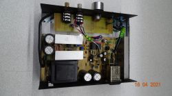
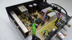
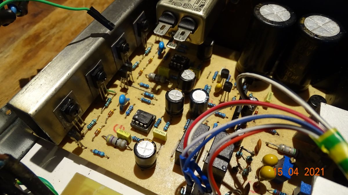
The power supply is built around the LM723 (Motorola) chip and the LF357 fast operational amplifier. Both circuits control a pair of power transistors on which heat is deposited. Filter Capacitors: 4 X 4700uF. Power supply of the entire amplifier set to 2 X 21V PR with PR - very stable power supply. There is no difference between the magnitude of the positive and negative voltage - maybe a 10mV difference. Trafo 2 X 0.44A sealed, soldered in PCB. Everything is protected by fuses, power supply with current limitation set at 0.3A. For filtering the power supply behind the stabilizer, I used tantalum and MUSE series capacitors. I did not want to make the power supply on the LM317 and its negative counterpart. The power supply on the LM723 and the operational amplifier, which makes sure that the negative voltage follows the positive voltage, is in my opinion better.
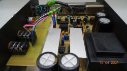
The protection circuit is an application of the NEC uPC1237HA chip. I started the circuit diagram with the kit from Advanced Electronic. The system delays turning on the headphones, disconnects them immediately after turning off the power, protects against DC component at the output, and protects against overload (clipping). The headphones are switched on with relays. The transistors cooperating with the circuit are low-noise. A failure / disconnection of the headphones is signaled by the LED diode. The parameters / protection time can be modified using discrete elements with the uPC1237 chip. A very good deal in my opinion.
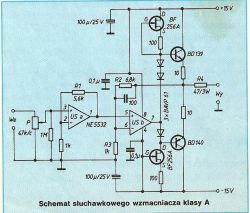
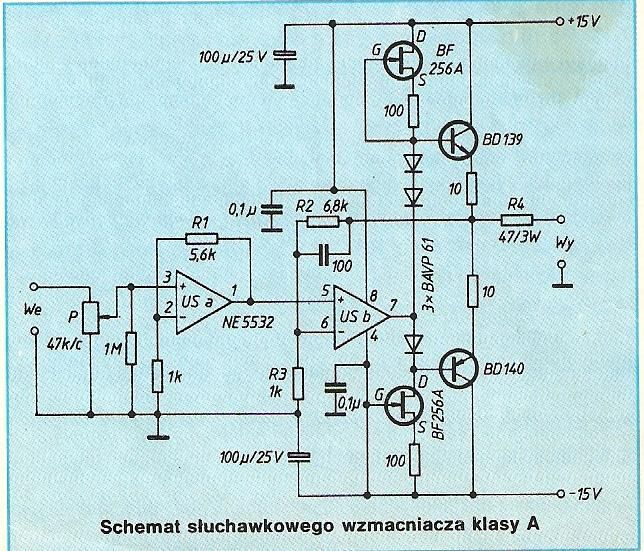
The power stage is based on a double operational amplifier and medium power transistors. The amplifier itself is the circuit presented in Elektora 10/93 (apparently it was originally described in the Dutch ELektuur, or the German Elektor). In my amplifier I used double operational amplifiers (two stages - pre-excitation and excitation stage in one circuit) LME49860 (by default they were NE5532), while in current sources I replaced BF256 transistors with newer 2Sk170 BL group (with increased Idss current compared to GR series). The author of the power level diagram mentioned about the 50mA quiescent current. I did not manage to achieve such a current - the current in my amplifier is about 38mA per transistor when powered by 21V (by the way, the magnitude of the supply voltage does not have much influence on the change of the Idss current). The 2SK BL group trnaistors have a higher current than the original BF256A. I reduced the resistors at the gates to 47ohm. I replaced the old BAY diodes with fast 1N-4151. The amplifier in idle state heats up strongly, the total quiescent current of both channels is not all 80mA. The system works with negative feedback. A power resistor is inserted on the output, which limits the gain and additionally protects (second protection) against short-circuit at the output. There is not a single capacitor in the amplifier circuit that would limit the frequency response. The appearance of the constant component is supervised by uPC1237. Paired JFET transistors - 0.5mA Idss difference, power transistors also paired - max 5% hFE gain difference. No output offset.
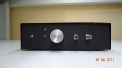
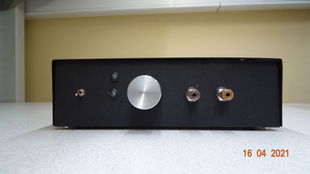
The front panel has an ALPS potentiometer (it was supposed to be a DALLAS DS1802 digital potentiometer, but it turned out that it has a problem with transferring more amplitude), two JACK Neutrik 6.3mm sockets, two indicators - one indicating the operation of the protection, while the other signaling the power supply and the switch.
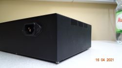
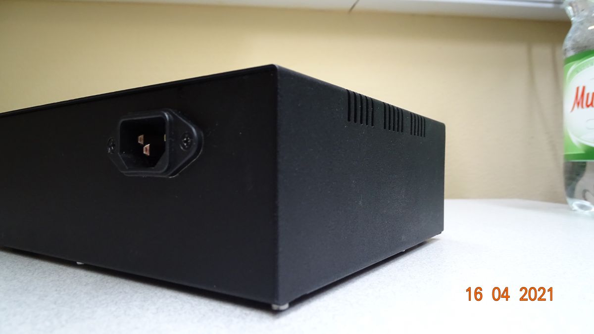
The whole is complemented by metallized resistors - where I could I stuffed tantalum capacitors, and the company's ELNA, MUSE etc. , filter on the 230V power input (found in the cabinet, new), fuse sockets on the PCB (three in total) universal metal housing.
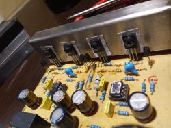
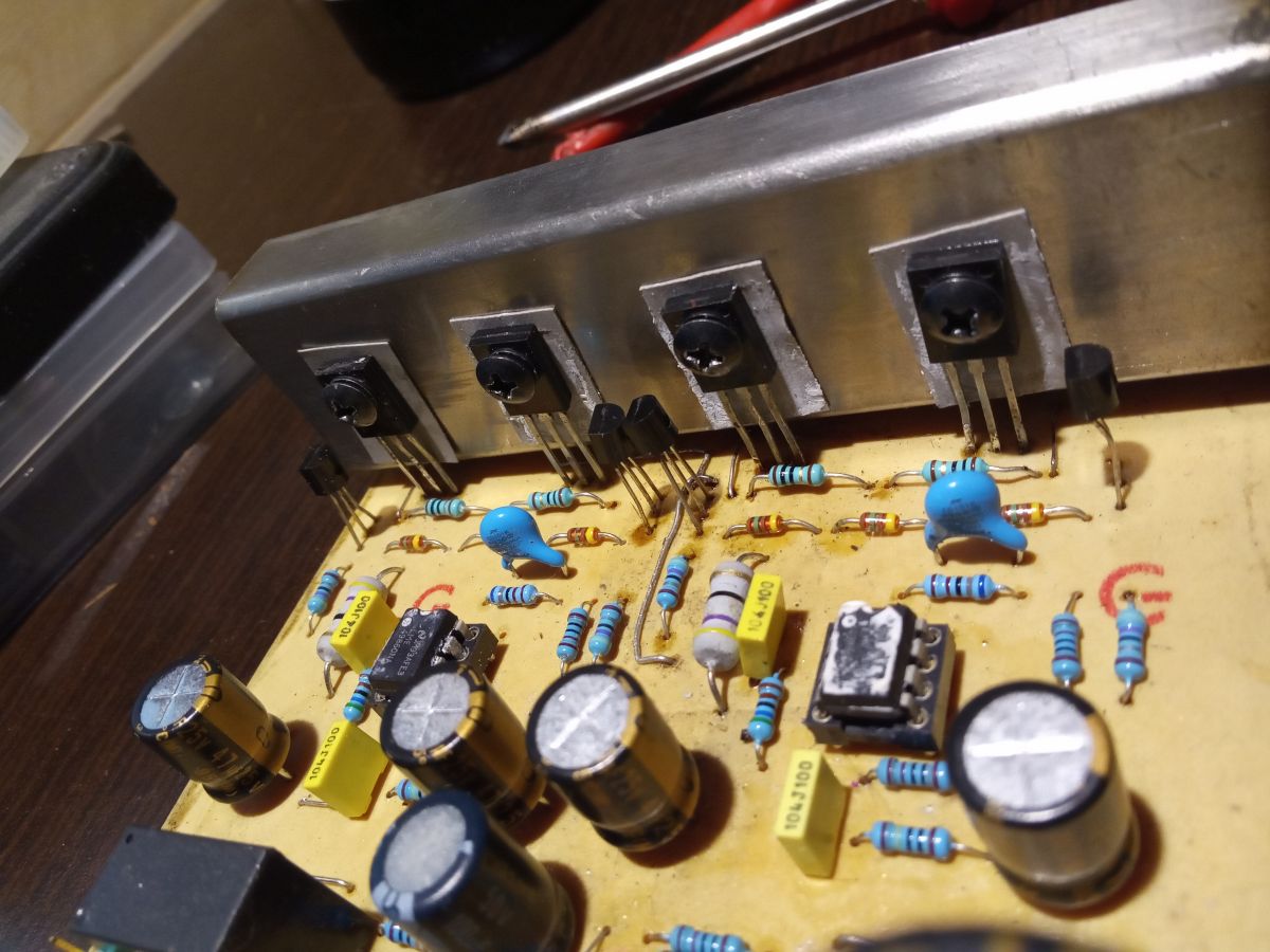
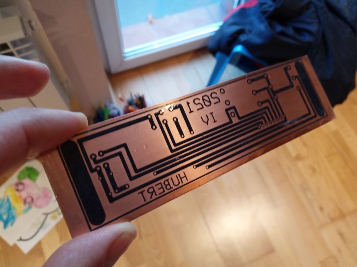
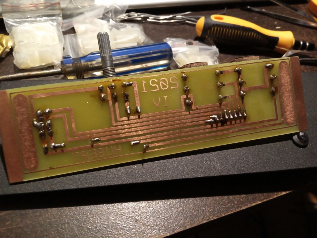
I made the PCB in the ExpressPCB program - unfortunately, despite numerous organoleptic checks, I made a few mistakes - I had to make a few changes, bridges on the PCB during soldering. I didn't have a PCB pattern for any of the schematics - everything was designed by myself. The board is made by thermal transfer on a thick - 1mm PCB. The bottom of the plate is secured with a solution of rosin and denatured alcohol (hence a bit of dirt on the upper side of the plate). The amplifier contains quite a lot of elements and thin tracks - all connections had to be made carefully.
I am positively surprised by the sound and sound quality of the amplifier. The amplifier sounds really beautiful. The gain is very high - you can limit it by lowering the sensitivity a bit (replacing one resistor). The whole thing took me a bit of work, but I am very happy with the amplifier. I generally tried to use good components. The stabilizer by MOTOROLA, an operational amplifier in a better class power supply, generally brand-name components.
Advantages of the amplifier:
- Enormous power - the amplifier will drive virtually any headphones
- Very little distortion
- Very nice sound
- Relatively simple options for making changes: gain, sensitivity, power, bandwidth, sound.
- Very good protection of the headphones - even in the event of burning the tips, failure of the power supply, clipping etc. the headphones will not be damaged
- Very low amplifier noise
- Everything is practically on one PCB
Disadvantages:
- Warming up of the whole
- Pretty complicated layout
- Lots of items
Planned changes:
- Replacing the potentiometer knob with one with a scale
- Heatsink enlargement - The heat sink used in the power stage is too weak
- Additional thermal protection of the power level
Amplifier:

Scheme of the power level and photos from the works:


Comments
Hello, Nice construction, well made. However, I have two comments: - the diagram in the output stage shows the complementary pair BD139-140, i.e. a push-pull amplifier in AB class, - there is a rule... [Read more]
Hello I wouldn't say that it is a class A amplifier, if you don't know what is going on inside the op-amps - they generally work in class AB. Case two - what about the damping factor? There is... [Read more]
And this cannot be solved by taking the feedback signal after the resistor R4 and not before? (i.e. from the exit). I recommend PCB varnishes - Plastik 70, Urethan spray. The design is very nice,... [Read more]
What is the power of trafo? It looks very small ... [Read more]
Hello The transformer has 20W ... 10W per secondary winding (444 mA at over 20V per winding). Of course, if we connect a 4ohm loudspeaker, the power supply will turn out to be too weak, but this is an... [Read more]
You can try to loop through the 47 ohm resistor. [Read more]
I would suggest to my dear colleagues to think about what influences the class in which this amplifier works, and how it can be easily changed (because you can easily maneuver between class A and AB).... [Read more]
E there, it seems to me that the D class can also sound well with headphones. However, there is a question why to do it - class D amplifiers have advantages in the form of high efficiency, say independent... [Read more]
In order to compare the systems, we use parameters, not feelings. [Read more]
It says in the topic that 38mA for one transistor, i.e. for the entire power amplifier (both channels), not all 80mA of quiescent current. 2SK170BL have a higher current than the BF256A mentioned in the... [Read more]
Only that the same current also flows through the second transistor, so it cannot be said that a current twice as large flows together. As for the class of the amplifier, it is rather class AB, but the... [Read more]
Yes - quiescent current per channel 38mA, let's round - 40mA quiescent current per channel. In my opinion, the amplifier sounds very well, the whole thing heats up very much [Read more]
What about temperature stabilization? Shouldn't these JFETs or serial diodes be somehow mounted on the heat sink together with the power transistors? At the moment, the only stabilization is provided... [Read more]
Therefore, I would change the resistors in the sources of these fets from 100 to 200 or even to 300. [Read more]
And what would it do? In the circuit from the original diagram, a current of about 2.25mA flows through the source resistors. Reducing this current will reduce the quiescent current in the emitter circuit... [Read more]
Well, I don't see any temperature feedback here. But since the final transistors do not go up with smoke after some time, it means that the current eventually stops at some value and still does not... [Read more]
The output USb at rest does not reach ground potential, only around -0.35V. This is because there are two LEDs on the upper half (Ubg = 1.4V) and only one on the lower half (Ubd = 0.7V). In total, there... [Read more]
there is a German standard DIN50332 (now European so EN) for the measurement conditions of headphones, which assumes that the headphones are powered from a signal source with a resistance of 120 Ohm! keyhole"... [Read more]
but the author complains that: So you have to decide whether this heating bothers him or not. But they still work in AB, depending on the quiescent current, only the 'depth' of this class... [Read more]