1. Introduction
Flyback converter is a buck-boost converter. It is one of the most popular topologies used to power devices with low power, has gained popularity thanks to its simple design and simple principle of operation. Many companies have added their solutions, improving some parameters; dynamic losses on the key were reduced, interference emission was removed from the optocoupler).
The principle of operation is very well illustrated by Wikipedia, so I will quote it:
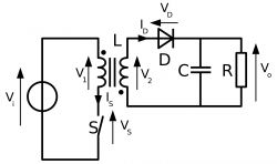
Fig. 1 Diagram of the flyback converter
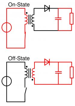
Fig. 2 Two operating states of the converter
The schematic of the converter is shown in Fig. 1. It operates on the principle similar to the buck-boost converter with a separated choke creating a transformer. When a continuous stream of magnetic induction in the reactor is maintained (continuous operation), two operating states can be distinguished:
- When the key is short (figure 2 at the top), the primary winding is connected to the voltage source. The current flowing through the primary winding and the magnetic flux in the core increases and the energy is stored in the transformer. The voltage on the secondary winding polarizes the diode. The output load is fed from the output capacitor.
- When the key is open (figure 2 at the bottom), the magnetic flux in the core decreases. The voltage on the secondary winding polarizes the diode in the direction of conduction and the current of the secondary winding flows through this diode into the load and the capacitor.
https://pl.wikipedia.org/wiki/Przekszta%C5%82tnik_flyback
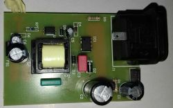
The schematic diagram is a simplified version that allows a better understanding of the principle of operation. The actual system is struggling with many problems that would not occur in an ideal arrangement, among others dynamic losses on the key, overvoltages on the primary winding, need for feedback or power supply for the controller. The following material is to bring closer the requirements regarding the power electronics equipment and problems related to PCB design. The material was created with the help of the user -RoMaN-, and the used controller is TNY280.
2. Tools and power electronics
Power electronics is a specialization that requires specific knowledge and equipment in relation to general electronics. You have to keep in mind that working with mains voltage is ALWAYS dangerous. Knowledge about protection against electric shock and awareness of what an error may end is mandatory.
In brief, I will describe what tools and equipment I used in this project.
Circuit Maker
As PCB design software, I chose Circuit Maker. This is a stripped down version of the Altium Designer program (Protel) available for free. It is a convenient tool for me with still great possibilities, a large database of projects and a connection to the base of Octopart elements. The latter is extremely useful, because if someone has already used the element we need, we will have a ready model, footprint and sometimes a 3D model, if we use the element as the first in the Circuit Maker community, we can create it by adding a brick. Many elements are made very well (which I consider to be a lot of plus Circuit Maker), however, a few have happened to me badly.
The project can be found under the link:
https://workspace.circuitmaker.com/Projects/Details/Kamil-Gulczuk/TNY280-flyback-12V-1A
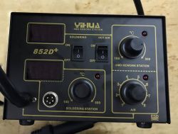
Equipment for power electronics
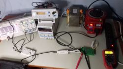
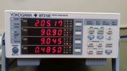
Figure 3. Equipment and station used to run and measure the power supply.
Separator transformer
This is one of the most important elements ensuring protection against damage to measuring equipment and, above all, our health. ALWAYS we supply the tested system with a separating transformer! We DO NOT CONNECT the oscilloscope to it! Why? Because we get rid of earthing from the oscilloscope housing which is unacceptable, because dangerous voltage will appear on the housing of the measuring device!
For advice on tinkering with the PE wire in the measuring device, I will give a warning!
Autotransformer
Sometimes it's worth to run the system from a lower voltage, for smaller sound-light effects, although it is not required
Reminder - the autotransformer does not provide galvanic isolation.
Such attention to the transformer and autotransformer.
The initial magnetizing current of the separating transformer and the autotransformer can be so large that it can release the overcurrent protection, which does not mean that the equipment is damaged. In order to avoid triggering the protection, I recommend using NTC thermistor in series.
Probes for oscilloscope
At high potential, we use x100 probes with 2kV DC isolation. Overvoltages in this type of systems can reach up to 1kV, and ordinary x10 probes can not withstand them and damage them.
Oscilloscope
Currently, the 100 MHz band is standard, but the usual 25 MHz is still sufficient for power electronics, because we operate on the first harmonic frequency up to 300 KHz rectangular waveform and multiplicity of the first harmonic. Of course, the better the frequency bandwidth, the more accurate oscillograms, but it is not that important.
Remeber! Oscilloscope channels are not usually isolated (in cheap oscilloscopes certainly are not) from each other, so we connect the oscilloscope ground probes to one point to avoid a short circuit.
Workplace
Personally, I have eternal mess on the desk, but the place where I run the system is to be ordered, clean and with insulated substrate (I use a polypropylene plate).Why? Damage to the system due to a lost resistor or tin ball lost somewhere under the circuit is as effective as it is frustrating.
3. Elements of the scheme
Why TNY280? It is an easy-to-design construction that gives a satisfactory final result.
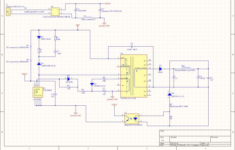
Figure 4. diagram
Looking at the schema at first glance, we see that it is much more complex than the overview scheme from Wikipedia. I will try to describe the individual functional elements in this diagram.
Snubber
The fundamental principle of operation of this topology is the accumulation of energy in a reactor with two (or more) windings, conjugated magnetic field. Unfortunately, not all of the stream is coupled with secondary windings, so during the process of key transition into the high impedance state, the energy accumulated in the inductance of dissipation looks for an outlet in the form of a current source, thus creating large voltage surges. To limit voltage surges, we use snubber. In the case of this project, I use the RCD snubber (RCD from the Diode Capacitor Resistor), which reduces the amplitude of the overvoltage and allows the energy to be lost from the dispersed inductance.
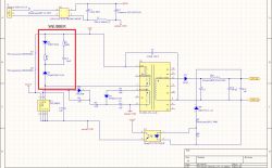
Figure 5. Snubber
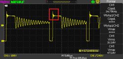
Figure 6. The course on the drain relative to GND. In the red frame, the vibration on the gauge.
feedback
The feedback in the case of TNY280 is implemented in the simplest way; when the voltage reaches the set value (Zener diode + Vf optocoupler diode) the EN / UV pin is shorted to GND and the controller switches off. It is a very simple solution in relation to eg changing the control signal fill, at the same time very effective at very low power and a good filter on the secondary side. Such a solution introduces much higher ripple voltage at the output, but simplifies the feedback to such an extent that we do not have to worry about whether our system will diverge (the system is always stable).
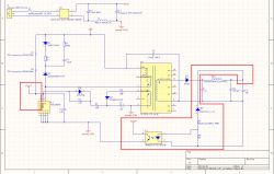
Figure 7. Feedback
Bias winding
In many controllers, the bias winding is responsible, among others, for the power supply of the controller, but in the case of TNY280 the system is supplied directly from the drain tubing, and the bias winding is optional. The use of bias winding in the case of TNY280 ensures reduced energy consumption at low load and the ability to configure overvoltage protection.
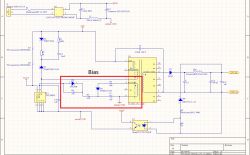
Figure 8. Bias winding
Transformer
When powering the device with mains voltage, special care must be taken and the transformer itself must meet the safety standards. If we do not have the knowledge and experience in winding transformers, I do not recommend doing it myself. The transformer used in the article was acquired at Feryster with the designation TI-EF20-12V-1A-W.
4. Measurements
Measurement of ripple at the output
Measurement of ripple and feedback are carried out directly on the output capacitor. In order to minimize the effect of signal attenuation through the loops of the oscilloscope probe itself, we use a silver-plated wire wound on the probe:
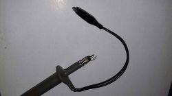
Figure 9. Probe with silver-plated wire.
Signals not measured in this way may look better (less ripple) due to the introduction of damping.
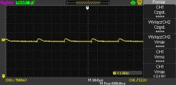
Figure 10. Ripples at the exit
Performance
Fitness is the parameter that we want to know next when we make sure that our system is working properly. Many beginners do not have wattmeters, thanks to which we can easily and in a simple way measure the power consumed by the power supply from the network.
Based on the material:
https://www.power.com/sites/default/files/PIU-102_MeasuringEfficiency.pdf
I will make three measurements with two equal meters
1. Measurement with the I-prober 520 current probe and the SDS1022DL oscilloscope
2 and 3 UT33C Multimeter
Figure 11. Measuring points.
For each of the measurements I use the same load - a 20 Ohm resistor. Current on load:
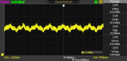
Figure 12. Current on load.
Distributed power on the resistor: 0.632 A * 12.11 = 7.654 W
Measurement first
The current probe is a very useful tool to visualize the current waveform in the system.
The measurements were made at two different alternating voltages: 230 V and 142 V
Results for 230 V
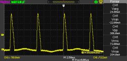
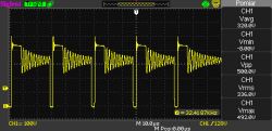
Figure 13. Current waveforms after the rectifier bridge for 230V
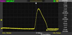
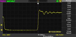
Figure 14. A single current pulse after the rectifying bridge for 230 V
Results for 142 V
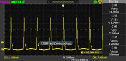
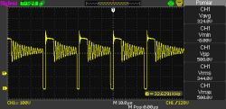
Figure 15. Current waveforms after the rectifier bridge for 142 V
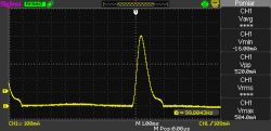
Figure 16. Single current pulse after rectifier bridge for 142V
I do not want to write down the calculations here, so I will give final results:
For 230 V - 97.6%
For 142 V - 86.2%
Measurement of the second
Made at the same point as the previous one, but with the UT33C multimeter. From the fact that in the picture of the alphanumeric display nothing is interesting, I will give only results:
For 230 V - 84.2%
For 142 V - 87.4%
Measurement of the third
-RoMaN- he instructed me to carry out the measurement in one more place, where the results will be more reliable. At this point, I also measured the UT33C multimeter.
For 230 V - 86.1%
For 142 V - 87.6%
Due to the poor quality of the oscilloscope and its resolution in the calculation of the average signal (4 mA) these results are completely irrelevant and have to be rejected, but the waveforms show very well that the peak current at a load of 7.65 W is for 230 V up to 284 mA ! I hope that this will help illustrate why PFC (power factor correction) systems are so important in pulse power supplies.
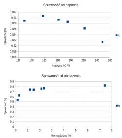
The remaining measurements look more credible, the only curiosity is the fact that the efficiency is better at the lower voltage supply. This is due to the fact that the increase in losses associated with conduction (diodes, copper resistance, leakage current of capacitors, etc.) is smaller than the increase in losses associated with the increase of supply voltage (dynamic losses on the key).
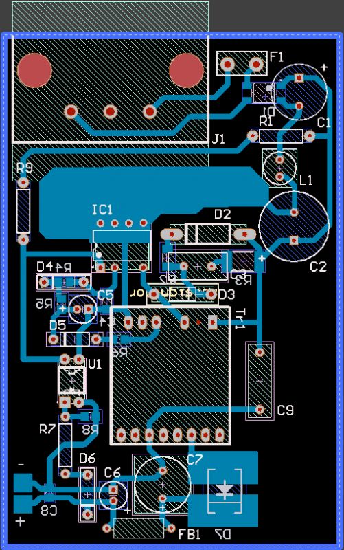
5. PCB
Implementation of the diagram is a very important stage in the design of the device, but the challenge is also the correct distribution of elements on the surface of the PCB. The scheme is considered as a set of ideal elements, where GND has the same potential everywhere. Unfortunately, the common error that I observe is the same GND treatment on the physical tile.
I will mention a few tips related to the physical placement of elements on the PCB.
1. Capacitors close to decoupling
Referring to the article about EMI interference:
https://www.elektroda.pl/rtvforum/topic3563554.html
When assembling elements on a PCB, we should keep current loops in mind. In the case of flyback we have two states: an open key and a closed key. In the first case, the current flows through the primary winding, the key and higher harmonics through the first capacitor:
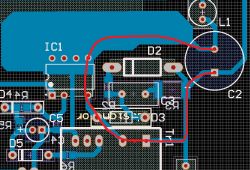
Figure 17. Current loop for the open key
In the second case, when the key ceases to conduct, the energy stored in the inductance of the transformer's dissipation is considered as a current source whose energy we need to dissipate on the gauge.
The red path shows the current flow in conditions when the energy is accumulated in the C3 capacitor, the yellow one shows the current loop flow through the transil if the surge amplitude is higher than the transil voltage (when the C3 capacitor accumulates too much energy).
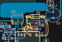
Figure 18. Current loop for a closed key
The purpose of a correct PCB design is to minimize the surface area of these loops. This can be accomplished even better by a double-layered PCB design or placing elements vertically.
2. Risk of puncture
When working with high voltage, we must remember that the distance between tracks - where there is a large potential difference - can easily be broken (creeping currents). The distance impact in which the breakdown occurs depends on the voltage, pressure, pollution, ambient temperature or shape of the electrodes. It's much easier to make a puncture in the blade-to-blade configuration, so we avoid guiding angular paths to minimize the chance of puncturing.
Depending on the working conditions and materials used, the gap between the tracks should be within 4mm to 12.6mm.
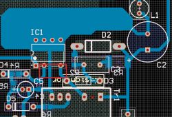
Figure 19. Intentionally unoriented path
Although in Fig.19 it would be wise to route paths perfectly between two neighboring ones, the shift is deliberately introduced.
3. Heat dissipation from elements (element dissipation power and heat sink)
A common mistake in beginners is a misunderstanding of the power dissipation parameter on the element. This parameter is given for very good (in practically unachievable conditions) heat dissipation by the heat sink. In the case of TNY280, we have two PCB surfaces that act as a heat sink (thermal pad) (232 mm ^ 2 and 645 mm ^ 2) for which thermal resistances are given (analogously 70 degrees / W and 60 degrees / W). In my case, it is a little over 300 mm ^ 2 and I do not overload the system over what the manufacturer gave me. Additionally, it is worth remembering that the barrier diode on the secondary side also has quite a lot of power, so it is worth to have a larger thermal pad.
It must be remembered that such thermal pads make it difficult to solder elements, because the power starts to dissipate on the heat sink, which makes it much harder to warm up the soldering point.
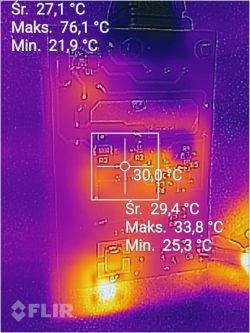
Figure 20. Photo from a thermal imaging camera. All PCBs
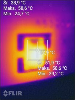
Figure 21. A picture from a thermal imaging camera. The diode on the secondary side.
6. Notes
I did the project completely for sport (experience is the basis), but I will share what mistakes I made:
- for small pads around THT elements, so that when I cut the wires a few pads fell off
- I forgot about test points, so I had to solder additional wires? for the derivation of elements
- one of the elements was badly designed and had a contour on the outline layer, which is milled by the machine - instead of a capacitor I would have a hole in the PCB, but during the verification of gerberas it was possible to notice and change it
- a few mistakes with element size and spacing (C3, C8 and C4)
These types of errors happen, so you can hardly assume that the first revision of the PCB will meet our expectations, so you have to assume at least 2-3 version of the PCB to get rid of all the failures.
7. Applications
Although the project can fail many people, because there is no calculation hererelated to individual elements (snubber, transformer, filters), but the purpose of this article was to show that, apart from these calculations, there are also many equally important steps at which many people make mistakes. To properly design the device, all steps must be performed correctly, if we make a mistake somewhere, the device will not work properly. It is worth limiting the number of places where we can potentially make mistakes by using the software provided by the manufacturer of the driver or commissioning items requiring precision to companies that have experience in this field. The smaller the field for error, the sooner you can diagnose the place where the mistake was made, so it costs us less time and nerves.
Cool? Ranking DIY


