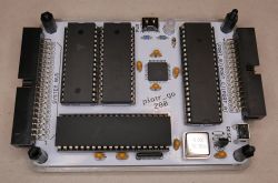
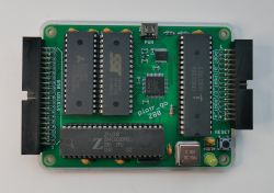
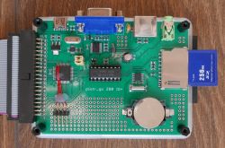
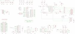
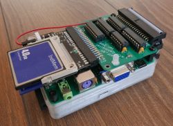
It was already 8051, now it's time for the Z80. The computer consists of several modules. The motherboard contains a Z80 processor, 512kB RAM and 512kB flash memory, IO 8255 chip and the Atmel ATF1502AS 5V CPLD that connects it all, which also works as a memory bank switch. The earlier version, instead of the Atmel chip, was based on the Xilinx CPLD and required an additional 3.3V-> 5V level converter. The "IO +" board is responsible for image generation, keyboard reading, sound generation, communication with the SD card and the clock. The required VGA, UARTa and YMZ284 clocks are generated by the Si5351 chip (configurable by I2C generator * 3).
Supported systems: CP / M, ZSDOS. 5V power supply via the USB-C socket.
Main tile and its earlier CPLD version of Xilinx: Z80, 512kB ram, 512kB flash, CPLD, 8255 IO.
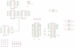
Diagram:
IO board: XC9572XL as uart, spi and interrupt controller. GD32 generates the image, reads the keyboard, configures the Si5351 and generates 50Hz to interrupt. YMZ284 sound generation. DS1302Z clock.
Congratulations on implementing an interesting project. Let me ask, have you carved your own BIOS for CP / M from scratch in Z80 assembly language? You made the so-called deblocking for SD card? Did you take any approach to CP / M 3.0?
I've been working on something like that for three years, too, but it's an 8080 project. It's also a much more retro layout. I even have FDD support and a completely self-written BIOS in 8080 assembly language. I also did deblocking for FDD. Other interesting facts include the LPT interface for the printer, the light pen and the RS232C mouse. The keyboard is also typical for a PC, but with a DIN connector. I also ran CP / M 2.2 and a whole bunch of period software. I am planning to add, among others stations 5.25 "in addition to the current 3.5".
As for the indicator devices, making the light pen is more difficult than it looks due to the jitter involved. This only works on the bright spots of the screen. However, even then, the effect is not always perfect. The mouse, on the other hand, works great. However, for this screen resolution, the transmitted shift must be divided by 2. I also wrote a simple "graphic" program in Pascal Mt +. I referenced additional BIOS functions that I did through assembly language snippets. The end result is quite good.
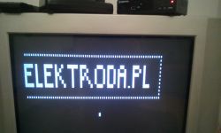
Start screen:
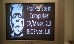
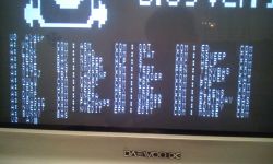
DIR command for USER 0:
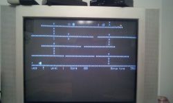
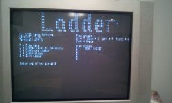
Ladder platform game:
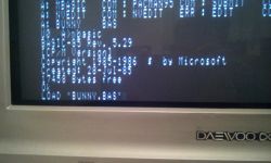
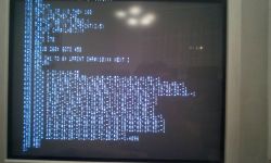
Microsoft BASIC and loading BUNNY.BAS (from the book "101 BASIC Computer Games"): Code snippet (LIST command): This program prints the Playboy bunny on a printer:

Effects of work in the MOUSE program that I wrote in Pascal MT +:
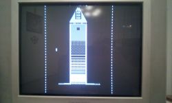
Terminal type change (one of the few extra commands I added to CP / M):
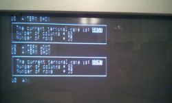
TINY BASIC for CP / M:
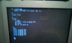
I also had fun with the muMATH program, which also appears as muSIMP: It is something like a modern MATLAB / SCILAB / OCTAVE-style environment for CP / M. It has really big possibilities, e.g. differentiating formulas, integrating (indefinite integrals) etc.
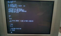
Light pen:
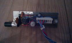
Motherboard:
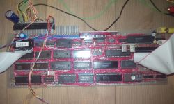
General view of the whole:
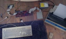
Generally, as you can see, the image is quite good and legible. However, a lot depends on the TV (band of the vision amplifier, screen diagonal, overall tuning - convergence, sharpness, geometry, etc.).
you carved your own BIOS for CP / M from scratch in Z80 assembly language?
Probably I would have done that, except that I had not dealt with the Z80 or CP / M before. I modified these sources: https://github.com/wwarthen/RomWBW The Z80 assembly language looks nicer than that of the C51. I think I will leave FDD for the FPGA version (if it is created). I am letting go of CP / M 3.0 for now.
The Z80 assembly language looks nicer than that of the C51.
A disputable statement. The instruction list in the Z80 as well as the entire processor is an extension of what was in the 8080. There is a huge archaism, such as conditional subroutine call or conditional return from subroutine. In the case of the 8051 it was a bit better, because such complex orders had already been removed. Haven't you thought about the modern EZ80? According to the documentation, it is compatible with the Z80, so also with the 8080.
piotr_go wrote:
I think I will leave FDD for the FPGA version (if it is created).
It's hard to do FDD. It's not easy to write a good driver. There is not only deblocking (emulating logical 128 B sectors on physical 512 B sectors), the skew table (without this, writing and reading are fast otherwise), etc.
piotr_go wrote:
I am letting go of CP / M 3.0 for now.
I'm not going to run this either.
I also made banks in my project. I have approx. 160 KB of RAM and 32 KB of ROM. CP / M is being loaded from EPROM right now. I also made a RAM DISK about 80 kB.
I think I will leave FDD for the FPGA version (if it is created).
Do you know if there is any open core FDC for 3.5 inch FDD? I searched and did not find. As with connecting FDD to FPGA in general, the outputs can be on 3V3 or must they be via a level converter? Ordinary resistors are enough for the inputs to prevent the FPGA from burning? I understand that most 3.5-inch FDDs do not require a 12V power supply and only 5V is enough to make it work.
By the way, this is an interesting FPGA project: http://searle.x10host.com/Multicomp/index.html Modular retrocomputer. Even if someone does not know VHDL (I prefer Verilog there), it can stick together. On this basis, I made a VGA terminal for a programmable calculator, it was only necessary to replace the ROM (implemented in the FPGA block frame) with my own. The problem is that with the EP2C5T144 chip, only 2kB of RAM is left (because 8kB eats the basic ROM, the rest is eaten by the generator's character memory).
It's hard to do FDD. It's not easy to write a good driver. There is not only deblocking (emulating logical 128 B sectors on physical 512 B sectors)
You can always do 128B sectors :)
fotomh-s wrote:
Do you know if there is any open core FDC for 3.5 inch FDD? I searched and did not find.
I wasn't looking for it, but it probably is, I wrote mine for the amiga.
fotomh-s wrote:
As with connecting FDD to FPGA in general, the outputs can be on 3V3 or must they be via a level converter? Ordinary resistors are enough for the inputs to prevent the FPGA from burning?
I did this: FPGA from left, flopp from right.
fotomh-s wrote:
I understand that most 3.5-inch FDDs do not require a 12V power supply and only 5V is enough to make it work.
A very nice design. Nice to see what miracles you can do with old procks :)
@piotr_go , of course, I have a few questions Are you satisfied with the Si5351? What is the role of T1 in the 8255 chip? What is this interrupt that requires 50Hz? (I've never had a Z80 in my hands)
Once again, congratulations on a nice project and I wish you continued success.
@piotr_go , @ maciej_333 How do you have an "organized" data bus in your projects? I wonder what happens when we give an address on the address bus to which nothing is attached and cpu will want to read the data. Do you have any way to keep the data bus low in this situation?
I wonder what happens when we give an address on the address bus to which nothing is attached and cpu will want to read the data. Do you have any way to keep the data bus low in this situation?
@piotr_go , @ maciej_333 How do you have an "organized" data bus in your projects? I wonder what happens when we give an address on the address bus to which nothing is attached and cpu will want to read the data. Do you have any way to keep the data bus low in this situation?
There is no need. Something like this has never been done. Anyway, in my case, all the space for data is used. In the case of the I / O space, there are free addresses for possible further expansion. In general, the program must be written in such a way that there is no reading / writing to unused areas, and even more so that the code is not executed from such a place.
You can give pull down resistors on the data bus, then when the PC is set to the address where nothing is there, it will perform NOPs.
maciej_333 wrote:
There is no need. Something like this has never been done.
True, I have not heard of anyone using this. However, the idea itself is not that bad, after all things can happen and programming errors can lead to a situation where the PC is set in an unused address space.
On FPGA you can combine it and, for example, make logic that will reset the core when reading or writing in the unused address space. On the actual hardware, such a combination is pointless.
You can give pull down resistors on the data bus, then when the PC is set to the address where nothing is there, it will perform NOPs.
Average idea. These resistors will load the data bus permanently. The permissible current Ioh is much smaller than the Iol. This is not always possible to afford. The 8080 and the Z80 are von Neumann architecture. If you use the unused space as data or a stack, the system will hang anyway.
fotomh-s wrote:
maciej_333 wrote:
There is no need. Something like this has never been done.
True, I have not heard of anyone using this. However, the idea itself is not that bad, after all things can happen and programming errors can lead to a situation where the PC is set in an unused address space.
The idea itself is not bad. However, this requires additional hardware chips. The hardware upgrade can therefore be quite significant. It would only make sense in a development system such as the native RTDS8.
As I wrote earlier, you have to write the program in such a way that it is not needed. Modern systems also do not have such protections.
I asked about such a solution because a similar mechanism is used in the ISA architecture and I would like to use it in my projects, but I don't know how to do it (I'm playing with MOS 6502).
As for the ISA architecture, the data bus is pulled high, which makes it possible to search the memory for tags and make sure it does not find any garbage. When the computer boots up, one of the POST tasks is just searching a certain area of I / O memory for the sequence of 55h and AAh bytes. If this string is found, it means that the expansion card ROM (which contains the program code to run) has been found.
What do I need this for? I dream of such a plug and play substitute
Hello I used to play CP / M in Amstrad with 3 "disk drives, due to the poor availability of floppy disks and their high price, I tried to connect the 5.25" station with average results. The station worked perfectly, but sometimes the original station (I was working on two) liked to go too far and jammed, you had to help it with your finger to get it back to the Home position. I do not remember if I was able to run the 3.5 "station, because the controller (used in the PC XT) did not support 1.44MB as far as I remember. Because it probably supported 720KB, I was looking for stations that had a pin to switch the station to 720KB mode. Amstrad 8256 had natively 3 stations "720KB. From the old days I was left with a disk controller for Amstrad 644 and an original book with descriptions and sources for CP / M +. By the way, this is the second CP / M I have been encountering recently, the first one of some Russian was on Atmega. It's a pity that the floppy disks have melted somewhere because I had Pascal, C and Forth about the databases have not been forgotten, DB probably version 2.2 best regards
Hello I'm in the process of building a simple z80 computer. I have one question about z80 addresses. It is about connecting the eeprom km28c17 or km28c64a systems with 12 addresses and 8-bit data bus to the address line. Everything was going well until the 11 address line eproma was connected to the 16 address line z80, what about the other addresses or the rest, i.e. A12, A13, A14, A15 will be unused? Give 10 k to the rest of the mass From A12 to A15?
with other addresses or the rest, i.e. A12, A13, A14, A15, will be unused?
It's best to connect to the address decoder, e.g. 74138, then the memory area will be divided into banks, in one you will have your eeprom and connect it with 'CE' to the '0' output so that it is addressed from '0', which will allow you to start z80. And the framework which he will also need links to the data and address lines and the 'CE' to the next number (bank) with '138' then the addresses will not overlap and interfere with each other. So, to sum up, km28c64a has 8kB, i.e. the entire address space with 80 can be divided into 8 blocks, just as much as can address 74138, to get this you connect A0- A12 with z80 to memory, Z80-74138 A13 - 1 A14 - 2 A15 - 3 -MREQ - 4 mass - 5 + 5V - 6
from 74138 to memory 15 - -CE you still need to 'multiply' the -RD, -WR signals with -MREQ to get the RD and WR signals for memory.
There is a lot of material on the web about building a simple computer on the z80, but the most interesting and practical are either in Arabic, English, Hindu or Urdu. Some people are unable to convey knowledge without passing the language barrier. I am not interested in building a structure on an arduino because it is an easy way. I have multiple Zilog chips and want to use them later. Today I have already covered a bit on the subject. Hardware works with80 + eeprom km28c17 simple assembly instructions. Everything, of course, on the contact plates.