logo elektroda
logo elektroda
X
logo elektroda

Changing firmware increasingly difficult? Smart Switch on T34 and QFN soldering

p.kaczmarek2 1602 25
ADVERTISEMENT
This content has been translated flag-pl » flag-en View the original version here
📢 Listen (AI):
  • T34 module in LGA package with fine wires soldered to pads
    There are an increasing number of backplane relay modules on the market based on the T34 chip. The T34 is an integrated Wi-Fi chip that is a smaller version of the popular CB2S/CB3S/itd based on the BK7231N core. Although it is still the same chip from the software side, changing its software is more difficult, because in new devices there is no longer a derived serial port and you have to solder this chip in the LGA case off the board. Here I will try to show this process.

    Let me remind you of the main topic about the T34: T34 datasheet, pinout, flashing and common mistakes - soldering to QFN pins, smart plug
    In that topic, the T34 occurred in a version where you could solder wires to its pads:
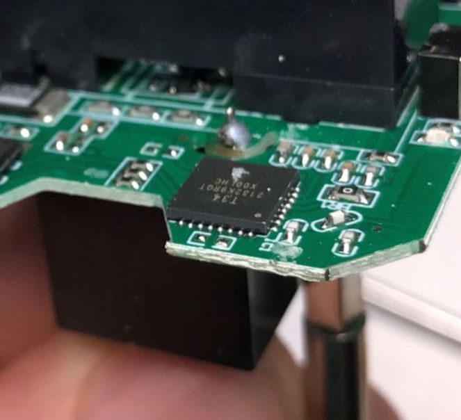
    Close-up of T34 LGA chip soldered to green PCB circuit board
    Here it will be more difficult - access to the pads is not available! This means that we no longer have a "shortcut" and we have to solder the whole T34 off the PCB, and after programming it has to go back in place.

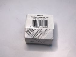
    This topic will be special, because I will show it on the example of two relays. This type of gadget can be bought for as little as a dozen zloty, you get a tiny box:
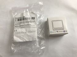
    Plastic packaging and cardboard box of Tuya WiFi relay module Box of KAMGA device labeled Intelligent flush-mounted WiFi switch
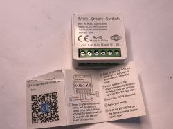
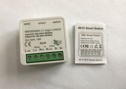
    There is a module and instructions inside:
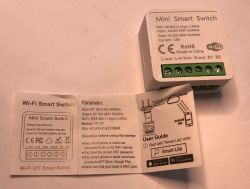
    Wi-Fi Mini Smart Switch with English-language instruction manual Mini Smart Switch with quick start guide and QR code for Smart Life app Wi-Fi relay module and instruction sheet with labeled connectors and specs
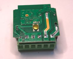
    Let's take a look inside:
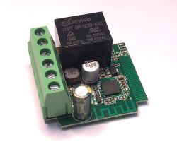
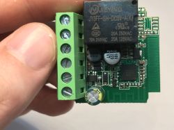
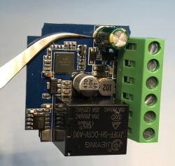
    Green PCB with visible traces, terminal block and soldered components. Remote relay module with green terminal block and black JY3FF relay Electronic circuit board with relay and screw terminal block in close-up
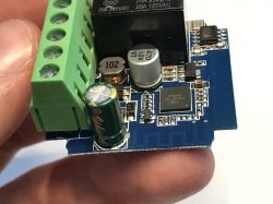
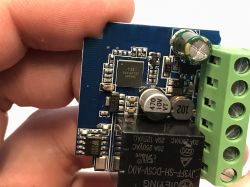
    Electronic module with relay, capacitors, and screw terminal Close-up of a blue PCB with electronic components and a green screw terminal Electronic module with relay, capacitors, and screw terminal block
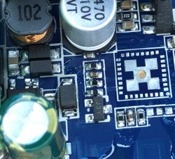
    There is no access to the pads mentioned in the subject line about T34 catalogue note .
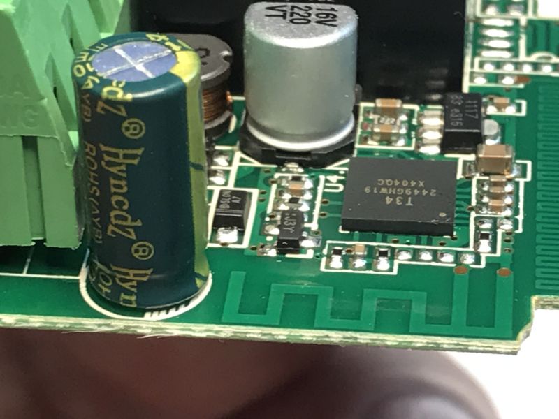
    Close-up of T34 Wi-Fi module on PCB with capacitor and SMD components
    We'll have something on this in a moment, but the construction of such a module can still be discussed briefly.
    Here we have a single relay supplied with 5 V (JY3FF-SH-DC5V-A(K) or similar), a step-down converter providing 5 V from 230 V AC (after rectification), probably on a BP2525, an LDO AMS1117-3.3 providing 3.3 V from 5 V, and a title T34 together with an antenna on the PCB. In addition, some of these modules also support an RF control option thanks to an additional WF480RA IC in the corner of the PCB along with its quartz resonator and antenna.

    ADVERTISEMENT


    Programming the T34
    The purpose of changing the device's firmware is to free it from the cloud and to pair it conveniently with Home Assistant. Such a device can then also be freely programmed and developed like an Arduino.
    We will upload our electrode firmware onto it: https://github.com/openshwprojects/OpenBK7231T_App
    Uploading is done via the serial port.
    Verification with the datalogue note shows that one of the UART pins needed for programming is not brought out here. You need to apply flux, ideally also protect nearby components with kapton tape and solder the T34 using hot air. The temperature and blow settings depend on the station - I always try to limit the blow, the temperature is not needed too high either. The board is small and has little heat capacity, it's not a big multilayer PCB from a laptop with huge copper spouts.
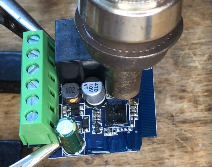
    Electronic module with T34 chip heated by hot air soldering station nozzle
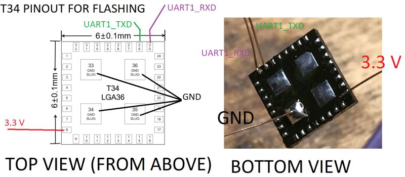
    GPIO download:
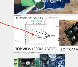
    T34 pinout diagram and photo with UART wires soldered for flashing
    After soldering, it can be seen that the TXD1 pad has no path:
    Close-up of relay PCB with desoldered T34 Wi-Fi module in LGA package Close-up of a PCB with removed LGA chip and visible QFN pads
    This way we have the module soldered out. I necessarily advise against soldering thick wires to it - it is easy for it to tear off the pad, I have already been through this, I broke one circuit myself this way. It is better to make a stand, e.g. from a cardboard box, mark the first pin and then fix the wires to the stand (e.g. with hot glue) and solder to them:
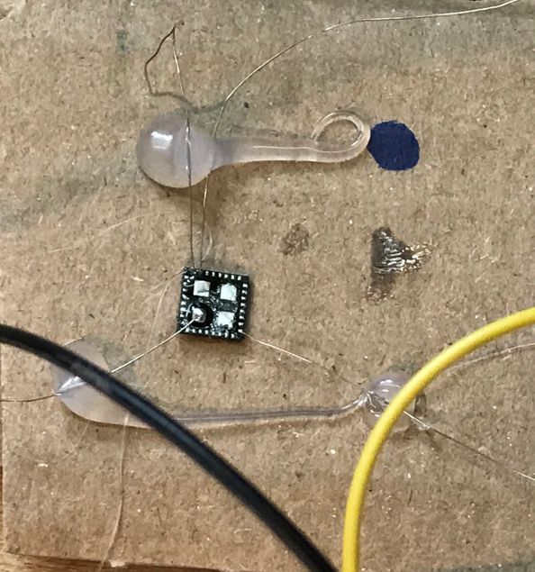
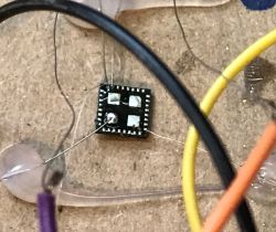
    T34 chip mounted on cardboard with thin wires soldered to its sides
    You can also buy a QFN breakout board with a compatible number of pins and raster. I didn't have one on hand myself, but my method works too - I even took a souvenir photo while reading the Flash memory:
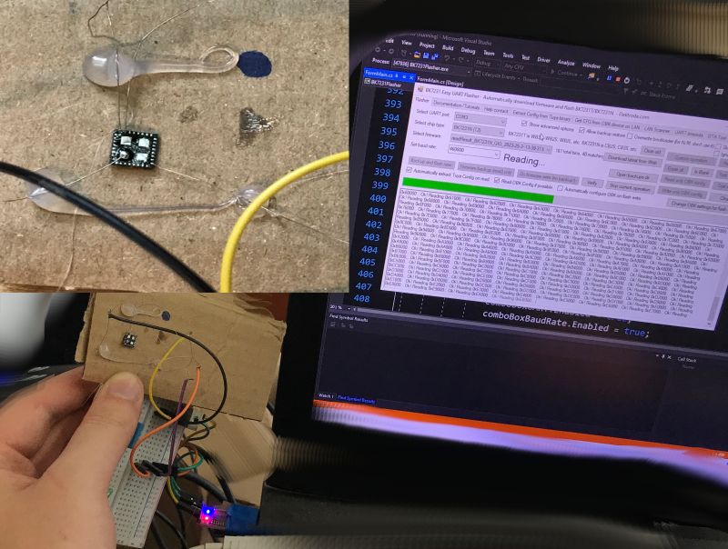
    T34 chip on cardboard with soldered wires, flashing tool software visible on screen
    Another copy - another risky method, but again, wires to not break the pads:
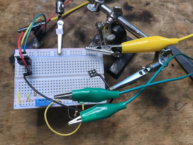
    Desoldered T34 chip connected to a breadboard with alligator clip wires
    We use our flasher and USB to UART converter for programming:
    https://github.com/openshwprojects/BK7231GUIFlashTool
    The programmer correctly discovers the GPIO configuration:
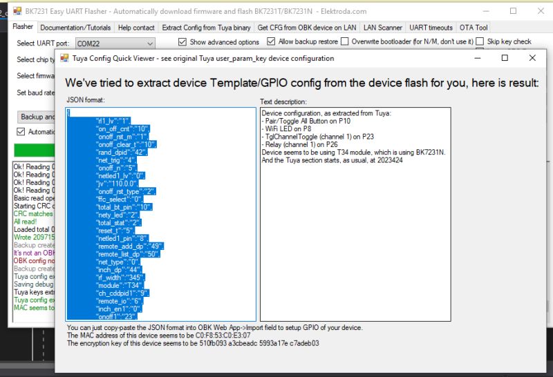
    Screenshot of BK7231 GUI Flash Tool showing extracted T34 GPIO configuration
    Then the chip goes back into place:
    Relay module with QFN-packaged T34 chip held in hand
    I do not reapply binder to such a layout. I just add a bit of flux, not too much, position it and heat it with hot air. With a bit of luck the layout sits and positions itself correctly. Sometimes it needs a little help with tweezers.

    Tuya's JSON detected (GPIO configuration):
    Code: JSON
    Log in, to see the code

    Verbal description:
    
    Device seems to be using T34 module, which is BK7231T chip.
    - Relay (channel 1) on P26
    - WiFi LED on P8
    - TglChannelToggle (channel 1) on P23
    - Pair/Toggle All Pin on P10
    

    We perform the rest of the configuration as usual.


    Pairing with Home Assistant:


    Summary
    Unlike the previous thread about the T34 , this time the conclusion is different. This device is unlikely to be reprogrammed without using hot air - because how? Does anyone have any ideas? Without the derived pads, I don't see this as a possibility.
    All this means that now having such, say, 5 modules, we have to solder the chip in the LGA 5 times, solder the wires to it, program it, and then solder it back in place.... well, at least a bit more people will practice working with SMD components.
    Is there any way to make your job easier? There was one suggestion on Elektroda.com:
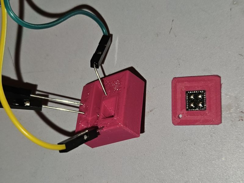
    Pink 3D-printed adapter with pins and desoldered QFN-package T34 chip on a surface
    This is a printed adapter for programming the T34 without soldering. It simplifies the second step, as the T34 has to be further soldered and re-soldered from the PCB. Source: https://www.elektroda.com/rtvforum/viewtopic.php?p=21732349#21732349
    Interesting concept, although it still requires probably the most difficult step.
    How do you rate the level of difficulty of such a firmware change? Have you worked with components in enclosures such as LGA?

    Cool? Ranking DIY
    Helpful post? Buy me a coffee.
    About Author
    p.kaczmarek2
    Moderator Smart Home
    Offline 
    p.kaczmarek2 wrote 13211 posts with rating 11031, helped 611 times. Been with us since 2014 year.
  • ADVERTISEMENT
  • #2 21737271
    piotr_go
    DIY electronics designer
    LGA not QFN.
  • #3 21737291
    Mastertech
    Level 28  
    Well, I don't know. To hook up to ground and plus you will probably find somewhere on the pcb. The question is whether the Rx and Tx go somewhere on the pcb so you can catch them, you need to look closely at the photo with the soldered circuit.
  • #4 21737307
    p.kaczmarek2
    Moderator Smart Home
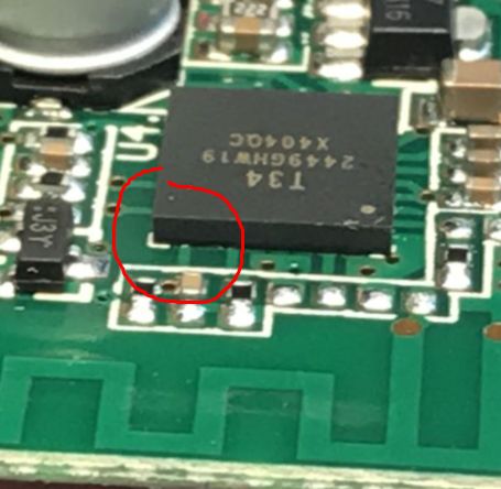
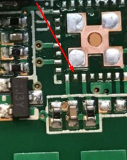
    Precisely the problem is that one of the UART lines is not led anywhere. That's why I gave pictures with the circuit soldered out:
    Close-up of QFN chip on PCB with exposed pads, one area marked with red circle. Close-up of a PCB with an LGA pad unconnected, pointed by a red arrow
    So you have 3.3 volts, you have ground, and you have one of the UART pins too - but what about the other?

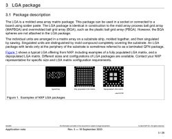
    As for the nomenclature, I'll have to check, as when I looked before publishing it didn't seem to fit me neatly with that LGA name, but I'm probably looking wrong.
    NXP documentation page showing LGA package description with three package diagrams
    "is sometimes referred to as a laminated QFN package"
    Helpful post? Buy me a coffee.
  • #5 21737367
    chemik_16
    Level 26  
    you can file in the circuit/pcb :)
    or press with a piece of tape
  • ADVERTISEMENT
  • #6 21737420
    piotr_go
    DIY electronics designer
    :) Darkest under the torch:
    T34 pinout diagram with TXD1, GND, and UART connections marked
  • ADVERTISEMENT
  • #7 21737429
    p.kaczmarek2
    Moderator Smart Home
    And that's what I saw, but about that I had doubts because I know that T34s come in two versions - with pads accessible from the side and without. Although I guess that document from NXP what I gave a screenshot earlier clarified the difference for me a bit, there it says that LGA with pads only at the edges, it is also called as "laminated QFN".

    So there are at least two types of this T34 - with or without "side" access.

    @chemik_16 I'll try it at the next switch. File the side of the chip?
    Helpful post? Buy me a coffee.
  • #8 21737477
    Mastertech
    Level 28  
    Why grind the whole side, just the corner where the pins of interest are, or in fact one particular pin.
    This will have the advantage that the access will be permanent and you will not have to solder again when you need to do the next programming.
  • #9 21737480
    piotr_go
    DIY electronics designer
    p.kaczmarek2 wrote:
    LGA with pads only at the edges, is also referred to as "laminated QFN".

    "laminated QFN" - as many as 15 links on google :)

    Since you are describing a problem that occurs in an LGA chassis and does not occur in QFN, it would be appropriate to write LGA.
  • #10 21737495
    p.kaczmarek2
    Moderator Smart Home
    I will try this way, but I do not foresee any further programming. That's what the remote update option (OTA) is for, to avoid soldering wires twice.

    @piotr_go thanks for pointing it out, I have changed it to be like in the documentation.
    Helpful post? Buy me a coffee.
  • #11 21737843
    divadiow
    Level 36  
    Was there any space under the chip for even the thinnest of needles to reach the IC legs? This method was a pain and you need to keep a steady hand for a short period but I was able to flash with two sewing needles carefully positioned with this device once:

    https://www.elektroda.com/rtvforum/topic4036975-60.html#21117203
    https://www.elektroda.com/rtvforum/topic4036975-60.html#21117908
  • #12 21737848
    p.kaczmarek2
    Moderator Smart Home
    @divadiow I checked your picture.
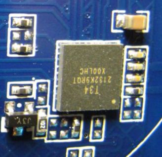
    Close-up of an integrated circuit on a blue PCB with SMD components
    It indeed looks like LGA (no pads on right side) but it seems it's solder in such a way that solder joins are still accessible. That was not the case for me. It seems that much depends on the board designer as well.
    Helpful post? Buy me a coffee.
  • #13 21737850
    divadiow
    Level 36  
    yep, OK. The accessibility of the legs on these T34s do seem to vary somewhat
  • #14 21737871
    p.kaczmarek2
    Moderator Smart Home
    Looks like the length of the pad makes the difference
    Helpful post? Buy me a coffee.
  • #15 21737924
    Nargo
    Level 23  
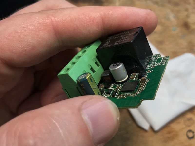
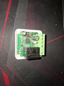
    Electromagnetic relay module with screw terminals on a PCB

    I have such a switch and am gathering up the courage.
  • #16 21738014
    Mastertech
    Level 28  
    You can easily add cables to it without desoldering the circuit.
    But placing it in the middle of the pcb doesn't make it any easier.
  • #17 21738061
    p.kaczmarek2
    Moderator Smart Home
    Now I'm wondering if the one in @Nargo's photo is a QFN, or is it also an LGA, but only on longer pads?

    Anyway, what's there is a simple version, also you could probably get away with such a stand with pins to embrace it.

    Or maybe there is just a UART brought out to the bottom of the PCB?

    If you succeed, @Nargo, remember that we are still collecting factory batches from the circuits (you can give on the forum as an attachment or give PR to us here: https://github.com/openshwprojects/FlashDumps ), and if our flasher detects a configuration, you can share the JSON + image and we'll add the entry to the list: https://openbekeniot.github.io/webapp/devicesList.html

    we have described (more or less accurately) 796 devices on the forum so far.
    Helpful post? Buy me a coffee.
  • #18 21740942
    _johnny_
    Level 9  
    Rest assured that soon no firmware changes in iot will be possible thanks to the EU. Every firmware will have to have a secure boot and on esp32, for example, the key is permanently burned in. Then only chip replacement will be an option.
  • #19 21740953
    p.kaczmarek2
    Moderator Smart Home
    At this point we have encountered this in devices from Matter based on ESP32. Several forum users have tested various such devices and it looks like this is some sort of top-down requirement from Matter, but I could be wrong.
    Sonoff M5-3C-80W light switch from Matter to ESP32 - can the firmware be changed?
    Helpful post? Buy me a coffee.
  • #20 21745590
    Atgeek25
    Level 2  
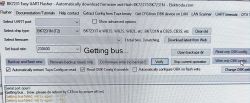
    I'm trying to flashing it, but I'm getting this error. Anyone knows why?
    BK7231 Easy UART Flasher interface showing bus connection errors
  • ADVERTISEMENT
  • #21 21746796
    p.kaczmarek2
    Moderator Smart Home
    This is not an error. You need to do a quick power off and on cycle, so it can "get bus".
    See guides for BK7231 here:
    https://www.youtube.com/playlist?list=PLzbXEc2ebpH0CZDbczAXT94BuSGrd_GoM
    Helpful post? Buy me a coffee.
  • #22 21747265
    rchristescu
    Level 7  
    If I try to polish the chip around TXD (Pin 26), where are the easiest accesses on the PCB for GND, 3.3V and RXD?
  • #23 21747317
    Atgeek25
    Level 2  
    >>21746796
    ok managed to solve it. Now the problem is that the module keeps disconnecting, sometimes works fine after a reboot, sometimes won't start again.
    Did anyone else experience the same problem with this module?
    Also, how do I tell which version to flash beetwen BK7231N and BK7231T? Ty
  • #24 21747363
    p.kaczmarek2
    Moderator Smart Home
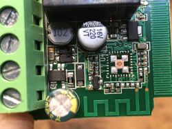
    @rchristescu see here, only one of UART signals has a pad that you can solder to:
    Close-up of a PCB with capacitors, an inductor, and screw terminals
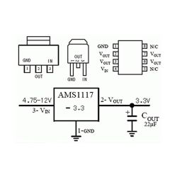
    For VDD and GND, see LDO pinout:
    AMS1117-3.3 voltage regulator schematic and package layout
    Interestingly enough, you can either choose 3.3V and solder to output of LDO, or you can use 5V and solder it to input of LDO, so there is still a safe 3.3V at the output. Just don't confuse pins! 5V may damage Beken.

    @Atgeek25 as in the first post - T34 is BK7231N . BK7231T is a different kind of Beken. If that's what you mean...

    How do you power it? Do you power it in circuit or did you solder it back to the PCB?
    Helpful post? Buy me a coffee.
  • #25 21747370
    Atgeek25
    Level 2  
    I resoldered it back

    Added after 55 [minutes]:

    I've tried different firmware as well, but the WiFi still randomly connect after a reboot
  • #26 21751338
    p.kaczmarek2
    Moderator Smart Home
    Please try 1.18.211 version, where we've applied WiFi stability patch.
    https://github.com/openshwprojects/OpenBK7231T_App/releases
    Also please make sure that you have "quick connect" disabled in flags.
    Helpful post? Buy me a coffee.
📢 Listen (AI):
ADVERTISEMENT