Eightree ET31 Smart Plug (BK7238 T1) Energy Monitoring: Teardown and flashing
TL;DR
- Eightree ET31 13A UK smart plug with energy monitoring uses a BK7238 T1 module and can be integrated with OpenBeken after teardown and flashing.
- The plug is solvent-welded shut, so opening it required heat, blades, clamps, and desoldering the main PCB to reach the hidden mini PCB and pins.
- The mini PCB exposes 11 staggered pins, including 3V3, GND, RX1, TX1, P24, P26, P6, P8, ADC, and CEN.
- BK7231 GUI Flash tool with BK7238 (T1) at 115200 backed up and flashed successfully, then the plug joined Wi‑Fi and exposed a web UI.
- Power metering looked inaccurate at first and may need calibration, and the LED no longer follows relay state by default.
Generated by the language model.
Eightree ET31 Smart Plug with Energy Monitoring 13A (BK7238 T1)
Note: loads of editing and moving parts here and there, so things might not be exactly spot on - if anything appears non-sensical, you will have to trust that it made sense before I cut/pasted the paragraph higher/lower. or not.
Description
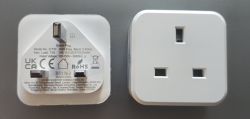
It plugs into a mains UK socket using the pins to the left in the picture below, then allows plugging in another device into the opposite end, to the right of the picture above.
You may then switch power off to the tethered device using the relay switch to the left side of the plug, as seen after plugging in. Also, after registering the device in the SmartLife app ("SmartLife - Smart Living" by Volcano Technologies Limited on PlayStore), you may connect the device to your account to trigger it remotely on demand, or on a timer or other events and to monitor power usage. You may then, also, connect the SmartLife account to your HomeAssistant instance for further integration - it works alright, just don't enjoy having to register them through another app. I knew this before purchasing, but have purchased it in hopes of being compatible with OBK, which I've found it was, only after cracking it open.
I have purchased it off here: https://www.amazon.co.uk/dp/B0B712GY64
I think I have paid some PLN30 for a pack of four, looks like it's cheaper now (PLN23.74).
"Disassembly"
It appears to be solvent-weld shut, so I could not open it without marring it (exploring less destructive ways of flashing).
A combination of flat screw drivers, stanley blade, precision crafts knife, clamps and heat was used to spread the seam around the protruding prongs.
After making a mess of it and ruining a few blades and my fingers, the assembly separated into the empty shell on the right below, and the electronics attached to the prongs, pictured left below.
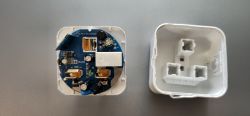
Once open I could see a mainboard onto which another board was attached, perpendicular to it, let's call it mini PCB. However, to access the pins, the board had to be taken out of the case.
After warming up and reshaping the plastic rivets out of the way(circled green below), I started by applying heat heavily to the N and L pads (circled red).
After many attempts with a desoldering pump and copper braid I've managed to wick out the solder from around the two joints, and was able to lift the main PCB out.
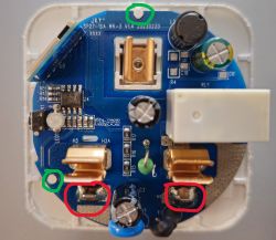
Some of the pin names were partially showing where the main and mini PCBs met, however, the rest of the pins were on the opposite side, covered by a shield, which had to come off the mini PCB.
Pins
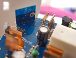
The mini PCB was sticking out through the bottom of the main PCB exposing 6 pins on the inner face, 5 pins on the outer face, in a zipper/staggered pattern between the two faces.
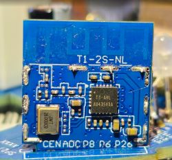
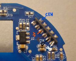
Preparations
Software
- BK7231 GUI Flash tool, running on my Windows 11 machine.
Hardware
- a long breadboard from this kit
- various Male-Male, Female-Female Dupont wires
- a FT232RL based USB to serial adapter (jumper configured to 3.3V)
- Soldering iron was a must, along with minimal amounts of flux and solder (unless you have spring pins and arms to make solderless contacts).
- a few rubber bands to help temporarily stabilise the PCB to the breadboard.
I have strapped the main PCB to a breadboard with rubber bands.
I then soldered some Dupont male to male wires to the pins underneath: 3v3, GND, RX, TX, CEN(opposite side).
I have connected the 4 wires to the breadboard: 3v3 to the positive rail, GND to the negative rail, RX, TX to their own ranks.
The 5th wire, CEN, was left loose for now; I will connect it to the GND rail at some point further down.
To each individual ranks I have added male to male wires (the serial adapter came with its own female to female dupont "loom").
I have connected RX(mini-PCB) to TX(serial adapter) and vice versa, then 3V3 to 3V3 and GND to GND.
I have connected the USB serial adapter to my computer and confirmed that the main PCB was powering up (LED switching on), I could hear the USB connection noise, which confirmed all good.
After launching the flash tool I could see that it was showing the correct COM port (confirm in Windows Device Manager).
Flashing
At this point there was a series of struggles either due to connecting the wire incorrectly, having a loose connection(before settling on my rubber bands + breadboard solution), setting the wrong chip type, baud rate. But I have eventually found that the below worked for me.
I have picked BK7238 (T1) as chip type and baud rate of 115200.
I was offered to download the latest firmware for the chip from the web; followed the instructions and was ready to flash.
If you click out of it, you can achieve the same with the button 'Download latest from Web'.
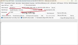
With the serial adapter powering on the mini PCB and hooked up to RX/TX, I have started the process.
After clicking 'Backup and flash new', the console started showing showing messages and it will also indicate it's time to trigger the device.
At this point I have connect the loose CEN wire to GND rail and kept it connected throughout the flashing process.
[size=12]I have read that you are meant to only touch CEN to GND for 0.25s at boot, but that did not work for me, however, keeping it solidly connected throughout worked ok.[/size]
It should start reading to create a backup, which can take between 3-5minutes, then move onto flashing the new firmware, which can take around the same amount of time.
If reading or writing stops and appears to not progress for extended periods of time, ensure that you have a solid connection on the wires - this is what drove me to strapping the thing to the PCB with rubber bands.
Once done, I got this screen showing some useful info which helped me configure the device after flashing:
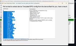
At this point I should have been able to disconnect the PCB and put it all back together - however, I kept mine strapped to the breadboard as I wasn't quite certain I was done needing access to the pins.
I have disconnected RX, TX and CEN from between the breadboard and the serial adapter.
Briefly disconnected the 3V3 and reconnected it to power up the board normally after flashing.
Walked away from it, but when I returned, I found a new open SSID I could connect to - sadly, I did not time it, so I cannot say whether it took 1 minute or 10.
Configuring
Once connected to the SSID, I went to http://192.168.4.1 and configured the device to connect to my intended SSID, and a backup SSID; saved and restarted.
I have located the device on my main network, and navigated to its config page (i.e. http://192.168.0.189/cfg) where I was able configure the module with the info shown to me at the end of the flashing process.
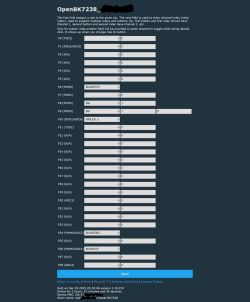
I have then restarted the device (disconnect 3V3, reconnected), saw the LED switched on, still connected to network.
Pleased with the result so far, so I've put it back together, just with tape as I suspect I might have to open it again in the near future.
I did not test the relay before putting back together, only after plugging back into mains.
I was able to switch the relay both from the WebUI and using the button built into the device.
Power meterage was a bit iffy, but might need calibration (my 90W iron went well above spec for a second, plug reported back ~126W then would stay at around 20W, possibly the cheap iron's fault, or maybe that's really it was drawing after reaching target temp, can't tell). However, I would get instant feedback when putting a load on, which I'm pleased with.
To import my setup, you may either mimic the settings above, or navigate to the web app page of the device (i.e. http://192.168.0.189/app?), switch to the Import tab, then paste my JSON (below) into field "1. Enter template here", followed by clicking "Clear OBK and apply new script from above".
Note: The factory behaviour of the device makes the LED follow the state of the relay. This changes after flashing. The default behaviour with OpenBeken is to have the LED as a WiFi LED. I have not worked out yet how to make the LED follow the relay state, but I will edit and add another JSON + other instructions once I do figure it out.
A less destructive way of doing this
I have 3 others I am looking to flash, but would prefer not to completely mangle the way I did this one.
Instead, I plan on cutting a slot that will expose the pins. Ideally, with a heated blade. Cutting it with a cold knife would set bits of plastic loose through the case.
Knowing the position of each pin, I hope I can simply poke the pins with needles through that slot. With Dupont wires soldered to each needle, I can then flash my device with minimal amounts of mangling.
I'm not quite there yet, but I'll share should this concept materialise.
I believe the size of the slot pictured below (to the right of the earth prong).should do as I can see all the pins looking straight down in.
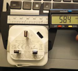
Hoping the picture below with a scale next to it will help align the cut better, should anyone decide to try this.
Measuring a non-mangled unit gives 58.1 mm height and width, whereas, the one I've messed with measures an extra 0.3mm (below).
Other measurements
These might not be needed now, but could help later:
Face: 57.1mm x 57.1mm (where you plug in the monitored device)
Rear: 58.1mm x 58.1mm
Depth from face to rear: 32.3mm
Dept from face to rear including the prongs island:39mm
Depth from face to tip of earth prong: 61.8mm
Distance from bottom edge of main body to bottom of the prongs island: 8.3mm
Distance from top edge of main body to tip of the prongs island: 6mm
Distance from left/right edge of main body to side of the prongs island: 5mm both left and right.
Width of the mini-PCB sticking out the bottom of the main PCB: 11.7mm
Thickness of the mini-PCB: 0.6mm
Spacing between pins: 1mm
Width of pins: 1mm
Note: loads of editing and moving parts here and there, so things might not be exactly spot on - if anything appears non-sensical, you will have to trust that it made sense before I cut/pasted the paragraph higher/lower. or not.

Description
It plugs into a mains UK socket using the pins to the left in the picture below, then allows plugging in another device into the opposite end, to the right of the picture above.
You may then switch power off to the tethered device using the relay switch to the left side of the plug, as seen after plugging in. Also, after registering the device in the SmartLife app ("SmartLife - Smart Living" by Volcano Technologies Limited on PlayStore), you may connect the device to your account to trigger it remotely on demand, or on a timer or other events and to monitor power usage. You may then, also, connect the SmartLife account to your HomeAssistant instance for further integration - it works alright, just don't enjoy having to register them through another app. I knew this before purchasing, but have purchased it in hopes of being compatible with OBK, which I've found it was, only after cracking it open.
I have purchased it off here: https://www.amazon.co.uk/dp/B0B712GY64
I think I have paid some PLN30 for a pack of four, looks like it's cheaper now (PLN23.74).
"Disassembly"
It appears to be solvent-weld shut, so I could not open it without marring it (exploring less destructive ways of flashing).
A combination of flat screw drivers, stanley blade, precision crafts knife, clamps and heat was used to spread the seam around the protruding prongs.
After making a mess of it and ruining a few blades and my fingers, the assembly separated into the empty shell on the right below, and the electronics attached to the prongs, pictured left below.

Once open I could see a mainboard onto which another board was attached, perpendicular to it, let's call it mini PCB. However, to access the pins, the board had to be taken out of the case.
After warming up and reshaping the plastic rivets out of the way(circled green below), I started by applying heat heavily to the N and L pads (circled red).
After many attempts with a desoldering pump and copper braid I've managed to wick out the solder from around the two joints, and was able to lift the main PCB out.

Some of the pin names were partially showing where the main and mini PCBs met, however, the rest of the pins were on the opposite side, covered by a shield, which had to come off the mini PCB.
Pins
The mini PCB was sticking out through the bottom of the main PCB exposing 6 pins on the inner face, 5 pins on the outer face, in a zipper/staggered pattern between the two faces.
| Inner | 3V3 |
| GND | | RX1 | | TX1 | | P9 |
| P24 | Outer | | P26 | | P6 | | P8 | | ADC | | CEN | |


Preparations
Software
- BK7231 GUI Flash tool, running on my Windows 11 machine.
Hardware
- a long breadboard from this kit
- various Male-Male, Female-Female Dupont wires
- a FT232RL based USB to serial adapter (jumper configured to 3.3V)
- Soldering iron was a must, along with minimal amounts of flux and solder (unless you have spring pins and arms to make solderless contacts).
- a few rubber bands to help temporarily stabilise the PCB to the breadboard.
I have strapped the main PCB to a breadboard with rubber bands.
I then soldered some Dupont male to male wires to the pins underneath: 3v3, GND, RX, TX, CEN(opposite side).
I have connected the 4 wires to the breadboard: 3v3 to the positive rail, GND to the negative rail, RX, TX to their own ranks.
The 5th wire, CEN, was left loose for now; I will connect it to the GND rail at some point further down.
To each individual ranks I have added male to male wires (the serial adapter came with its own female to female dupont "loom").
I have connected RX(mini-PCB) to TX(serial adapter) and vice versa, then 3V3 to 3V3 and GND to GND.
I have connected the USB serial adapter to my computer and confirmed that the main PCB was powering up (LED switching on), I could hear the USB connection noise, which confirmed all good.
After launching the flash tool I could see that it was showing the correct COM port (confirm in Windows Device Manager).
Flashing
At this point there was a series of struggles either due to connecting the wire incorrectly, having a loose connection(before settling on my rubber bands + breadboard solution), setting the wrong chip type, baud rate. But I have eventually found that the below worked for me.
I have picked BK7238 (T1) as chip type and baud rate of 115200.
I was offered to download the latest firmware for the chip from the web; followed the instructions and was ready to flash.
If you click out of it, you can achieve the same with the button 'Download latest from Web'.

With the serial adapter powering on the mini PCB and hooked up to RX/TX, I have started the process.
After clicking 'Backup and flash new', the console started showing showing messages and it will also indicate it's time to trigger the device.
At this point I have connect the loose CEN wire to GND rail and kept it connected throughout the flashing process.
[size=12]I have read that you are meant to only touch CEN to GND for 0.25s at boot, but that did not work for me, however, keeping it solidly connected throughout worked ok.[/size]
It should start reading to create a backup, which can take between 3-5minutes, then move onto flashing the new firmware, which can take around the same amount of time.
If reading or writing stops and appears to not progress for extended periods of time, ensure that you have a solid connection on the wires - this is what drove me to strapping the thing to the PCB with rubber bands.
Once done, I got this screen showing some useful info which helped me configure the device after flashing:

At this point I should have been able to disconnect the PCB and put it all back together - however, I kept mine strapped to the breadboard as I wasn't quite certain I was done needing access to the pins.
I have disconnected RX, TX and CEN from between the breadboard and the serial adapter.
Briefly disconnected the 3V3 and reconnected it to power up the board normally after flashing.
Walked away from it, but when I returned, I found a new open SSID I could connect to - sadly, I did not time it, so I cannot say whether it took 1 minute or 10.
Configuring
Once connected to the SSID, I went to http://192.168.4.1 and configured the device to connect to my intended SSID, and a backup SSID; saved and restarted.
I have located the device on my main network, and navigated to its config page (i.e. http://192.168.0.189/cfg) where I was able configure the module with the info shown to me at the end of the flashing process.

I have then restarted the device (disconnect 3V3, reconnected), saw the LED switched on, still connected to network.
Pleased with the result so far, so I've put it back together, just with tape as I suspect I might have to open it again in the near future.
I did not test the relay before putting back together, only after plugging back into mains.
I was able to switch the relay both from the WebUI and using the button built into the device.
Power meterage was a bit iffy, but might need calibration (my 90W iron went well above spec for a second, plug reported back ~126W then would stay at around 20W, possibly the cheap iron's fault, or maybe that's really it was drawing after reaching target temp, can't tell). However, I would get instant feedback when putting a load on, which I'm pleased with.
To import my setup, you may either mimic the settings above, or navigate to the web app page of the device (i.e. http://192.168.0.189/app?), switch to the Import tab, then paste my JSON (below) into field "1. Enter template here", followed by clicking "Clear OBK and apply new script from above".
Note: The factory behaviour of the device makes the LED follow the state of the relay. This changes after flashing. The default behaviour with OpenBeken is to have the LED as a WiFi LED. I have not worked out yet how to make the LED follow the relay state, but I will edit and add another JSON + other instructions once I do figure it out.
Code: JSON
A less destructive way of doing this
I have 3 others I am looking to flash, but would prefer not to completely mangle the way I did this one.
Instead, I plan on cutting a slot that will expose the pins. Ideally, with a heated blade. Cutting it with a cold knife would set bits of plastic loose through the case.
Knowing the position of each pin, I hope I can simply poke the pins with needles through that slot. With Dupont wires soldered to each needle, I can then flash my device with minimal amounts of mangling.
I'm not quite there yet, but I'll share should this concept materialise.
I believe the size of the slot pictured below (to the right of the earth prong).should do as I can see all the pins looking straight down in.
Hoping the picture below with a scale next to it will help align the cut better, should anyone decide to try this.
Measuring a non-mangled unit gives 58.1 mm height and width, whereas, the one I've messed with measures an extra 0.3mm (below).

Other measurements
These might not be needed now, but could help later:
Face: 57.1mm x 57.1mm (where you plug in the monitored device)
Rear: 58.1mm x 58.1mm
Depth from face to rear: 32.3mm
Dept from face to rear including the prongs island:39mm
Depth from face to tip of earth prong: 61.8mm
Distance from bottom edge of main body to bottom of the prongs island: 8.3mm
Distance from top edge of main body to tip of the prongs island: 6mm
Distance from left/right edge of main body to side of the prongs island: 5mm both left and right.
Width of the mini-PCB sticking out the bottom of the main PCB: 11.7mm
Thickness of the mini-PCB: 0.6mm
Spacing between pins: 1mm
Width of pins: 1mm


Comments
Thanks for sharing. So we're really seeing more and more of T1 (BK7238) chips these days. I guess 2026 will be the year of BK7238 :D I did it once for few plugs, but I can't say it went nicely for... [Read more]
Hi vargabp, great teardown, thank you. I had a few of these Eightree model ET31s too. Just to note for anyone following, although completely similar externally, the internals of the switch I chose to... [Read more]
That's certainly interesting, it would be useful to know if your revision distinguishes itself from the ones I bought without having to crack it open. Are the external markings any different? Is the shape... [Read more]
So the external form of the plug is the same with some different screen printing on the base (photo attached). It still identifies itself as an 'ET 31' and 'Etavost consulting' appear to have made the... [Read more]