I would like to introduce a simple design of a small inverter for a 3 phase motor with a power of about 400W.
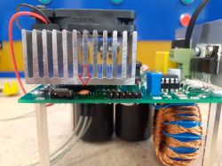
View of the inverter in the photos below
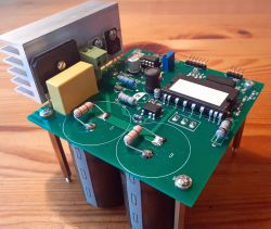
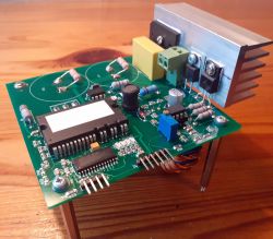
The inverter is powered from one phase, with alternating voltage 230 V. The output gives a 3-phase voltage 3x 230V. The inverter schematic, software, PCB design are in the attachments.
I think most of the readers who will be interested in this post know how the inverter works and what it is for. The reason why I built the inverter was the price of the main control element FNA41560, which on aliexpress is about 8 PLN. However, as it turned out later, the cost of the remaining elements was about PLN 200. The most expensive components are capacitors and a choke. So it's worth considering before you start building an inverter, because you can probably buy a ready-made one at this price. There is a PFC system at the inverter input, which ensures that the current drawn from the grid is not distorted and is in phase with the voltage. However, the degree of deformation depends on the load as shown in the pictures below

The voltage on the filter capacitors is approximately 430 V without load and drops to 400 V when the PFC is loaded. In the inverter, the transistors commutate at a frequency of 5kHz, because for this frequency the FNA41560 has been optimized, the dead times for transistors are about 1.2 us as in the pictures

The inverter has high temperature protection set at 105 ?C, 5 A short circuit, and high voltage on 460 V filtering capacitors. cycle by cycle mode, ie it automatically resets at the end of each PWM cycle (acts as a current limitation). This can be changed in the P1FLTACON microcontroller register to the "latch" mode. In the "latch" mode, the PWM generators turn off and stop until the marker is deleted. The frequency is regulated by a multi-turn potentiometer with a resolution of 0.1 Hz. Adjustable frequency range from 1 Hz to 80 Hz. The useful range starts at 5Hz. The VSM -space vektor modulation algorithm was used to generate the output waveform, which allows the maximum use of DC voltage supplied to the FNA41560 module. More details on this type of control can be found, for example, on the microchip page
https://microchipdeveloper.com/mct5001:space-vector-modulation
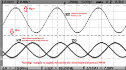
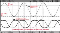
The differences in the shapes of the waveforms generated by SPWM and SVM are shown in the figures below. In the case of SPWM, the maximum phase-to-phase voltage at the inverter output can be at most ?3 / 2 x Udc in the case of SVM is Udc - if losses in transistors are neglected. In fact, the SVM method gives about 15% higher output voltage compared to the Sine PWM method.

It should be remembered that the power supply of the system is not isolated from the mains and special care should be taken during commissioning and use. The mass of the system in relation to the ground is potentially life-threatening .
However, if someone would like to build and run an inverter, below I am giving some helpful tips and attaching videos from commissioning. The sounds that can be heard are not generated by friction of the bearings or the ventilator, I do not know how they arise, I can only confirm that the motor connected to a 3-phase sinusoidal source does not generate them.
[movie: fdf5ab2e81] https://filmy.elektroda.pl/37_1601565891.mp4 [/ movie: fdf5ab2e81]
In the second video, between the inverter and the motor, I turned on the LC filter 3x L = 1.5mH and 3 x C = 0.68uF, which in my opinion made the sounds a bit quieter.
[movie: fdf5ab2e81] https://filmy.elektroda.pl/59_1601566389.mp4 [/ movie: fdf5ab2e81]
The assembly suggests soldering and then starting the PFC part, soldering the MC33262 integrated circuit, rectifier bridge, diode D11, Q1 transistor and choke, filtering capacitors C17 and C22 to which you need to solder 470 k? resistors to each one as in the picture. Winding (3 turns) should be wound on the choke, which will power the MC33262 integrated circuit. I used a cable from a computer network cable (so-called path cord) for winding it. The end and beginning of the windings are important and should be connected as in the application note. I used an inductance meter to determine the start and end of the windings. I connected the wound winding to the choke winding in series and compared the measured inductance values. In the case of obtaining a higher value of inductance, I obtained a connection between the end and the beginning of the windings. The power supply to the inverter should be led through starting thermistors to limit the current flowing through the D11 diode, and for which there is not enough space on the board, or to use another solution that will limit the inrush current. I used 2 NTC6D-15 thermistors with a maximum current of 5A. Direct connection to the mains may damage the D11 diode. After soldering the PFC circuit elements, I soldered two 100W / 230V incandescent bulbs connected in series to the capacitors, thus I checked whether the PFC works. The voltage on the bulbs should be 400V
The next step I made was soldering and checking the operation of the transformerless power supply built on the LNK306. At the output of which you should measure the voltage, which should be 15 V. At the very end, I soldered the FNA41560 and the microcontroller that should be programmed in the system. The J3 compatible Pickit3 connector is used for programming.
In order to start the system, apart from turning on the power, give logical number 1 from the RA2 output to the RA3 input, then the inverter starts up to the speed set by the potentiometer with the ramp for about 5 seconds. Connecting RA3 to ground causes the inverter to stop - the transistors are turned off.
It is important to control the starting or stopping of the inverter from the RA2 output (pin 1 on J4 as shown in the diagram) because in the event of too high temperature or other disturbances the state on R2 changes to low and the inverter turns off.
Noteworthy is the FVO output (pin 11) of the FNA41560 chipwhich is shorted to ground when the supply voltage is less than 12 V and also when the system is not powered. This is indicated by the fault diode, during the startup and initial tests, when the power supply from the pickit3 programmer is connected to the board, do not worry about it - you just have to remember that when this diode is lit on the microcontroller output, no PWM waveforms are generated.
To get rid of this error and get PWM waveforms at the output of the microcontroller, temporarily disconnect the power from the programmer and connect 15 V to the FNA41560. Of course, we only perform these activities when the inverter is disconnected from the power grid.
The maximum output voltage of the inverter is obtained at a frequency of 60 Hz.
For low frequencies, the voltage between 1 Hz - 5 Hz is constant. Above 5Hz, U / f = constant increases.
The system was assembled on a board with dimensions of 100 x 100 mm so that the cost of the tiles was $ 2.
The program was written in C in the MPLABX environment.
Finally, I would like to add that, apart from the starting thermistors, the inverter should be powered by an anti-interference filter.
View of the inverter in the photos below


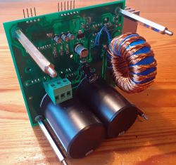
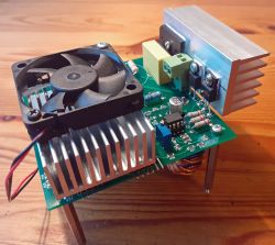
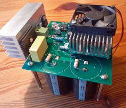
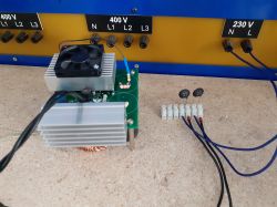
The inverter is powered from one phase, with alternating voltage 230 V. The output gives a 3-phase voltage 3x 230V. The inverter schematic, software, PCB design are in the attachments.
I think most of the readers who will be interested in this post know how the inverter works and what it is for. The reason why I built the inverter was the price of the main control element FNA41560, which on aliexpress is about 8 PLN. However, as it turned out later, the cost of the remaining elements was about PLN 200. The most expensive components are capacitors and a choke. So it's worth considering before you start building an inverter, because you can probably buy a ready-made one at this price. There is a PFC system at the inverter input, which ensures that the current drawn from the grid is not distorted and is in phase with the voltage. However, the degree of deformation depends on the load as shown in the pictures below
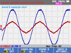
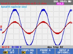
The voltage on the filter capacitors is approximately 430 V without load and drops to 400 V when the PFC is loaded. In the inverter, the transistors commutate at a frequency of 5kHz, because for this frequency the FNA41560 has been optimized, the dead times for transistors are about 1.2 us as in the pictures
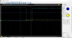
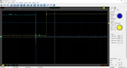
The inverter has high temperature protection set at 105 ?C, 5 A short circuit, and high voltage on 460 V filtering capacitors. cycle by cycle mode, ie it automatically resets at the end of each PWM cycle (acts as a current limitation). This can be changed in the P1FLTACON microcontroller register to the "latch" mode. In the "latch" mode, the PWM generators turn off and stop until the marker is deleted. The frequency is regulated by a multi-turn potentiometer with a resolution of 0.1 Hz. Adjustable frequency range from 1 Hz to 80 Hz. The useful range starts at 5Hz. The VSM -space vektor modulation algorithm was used to generate the output waveform, which allows the maximum use of DC voltage supplied to the FNA41560 module. More details on this type of control can be found, for example, on the microchip page
https://microchipdeveloper.com/mct5001:space-vector-modulation
The differences in the shapes of the waveforms generated by SPWM and SVM are shown in the figures below. In the case of SPWM, the maximum phase-to-phase voltage at the inverter output can be at most ?3 / 2 x Udc in the case of SVM is Udc - if losses in transistors are neglected. In fact, the SVM method gives about 15% higher output voltage compared to the Sine PWM method.
It should be remembered that the power supply of the system is not isolated from the mains and special care should be taken during commissioning and use. The mass of the system in relation to the ground is potentially life-threatening .
However, if someone would like to build and run an inverter, below I am giving some helpful tips and attaching videos from commissioning. The sounds that can be heard are not generated by friction of the bearings or the ventilator, I do not know how they arise, I can only confirm that the motor connected to a 3-phase sinusoidal source does not generate them.
[movie: fdf5ab2e81] https://filmy.elektroda.pl/37_1601565891.mp4 [/ movie: fdf5ab2e81]
In the second video, between the inverter and the motor, I turned on the LC filter 3x L = 1.5mH and 3 x C = 0.68uF, which in my opinion made the sounds a bit quieter.
[movie: fdf5ab2e81] https://filmy.elektroda.pl/59_1601566389.mp4 [/ movie: fdf5ab2e81]
The assembly suggests soldering and then starting the PFC part, soldering the MC33262 integrated circuit, rectifier bridge, diode D11, Q1 transistor and choke, filtering capacitors C17 and C22 to which you need to solder 470 k? resistors to each one as in the picture. Winding (3 turns) should be wound on the choke, which will power the MC33262 integrated circuit. I used a cable from a computer network cable (so-called path cord) for winding it. The end and beginning of the windings are important and should be connected as in the application note. I used an inductance meter to determine the start and end of the windings. I connected the wound winding to the choke winding in series and compared the measured inductance values. In the case of obtaining a higher value of inductance, I obtained a connection between the end and the beginning of the windings. The power supply to the inverter should be led through starting thermistors to limit the current flowing through the D11 diode, and for which there is not enough space on the board, or to use another solution that will limit the inrush current. I used 2 NTC6D-15 thermistors with a maximum current of 5A. Direct connection to the mains may damage the D11 diode. After soldering the PFC circuit elements, I soldered two 100W / 230V incandescent bulbs connected in series to the capacitors, thus I checked whether the PFC works. The voltage on the bulbs should be 400V
The next step I made was soldering and checking the operation of the transformerless power supply built on the LNK306. At the output of which you should measure the voltage, which should be 15 V. At the very end, I soldered the FNA41560 and the microcontroller that should be programmed in the system. The J3 compatible Pickit3 connector is used for programming.
In order to start the system, apart from turning on the power, give logical number 1 from the RA2 output to the RA3 input, then the inverter starts up to the speed set by the potentiometer with the ramp for about 5 seconds. Connecting RA3 to ground causes the inverter to stop - the transistors are turned off.
It is important to control the starting or stopping of the inverter from the RA2 output (pin 1 on J4 as shown in the diagram) because in the event of too high temperature or other disturbances the state on R2 changes to low and the inverter turns off.
Noteworthy is the FVO output (pin 11) of the FNA41560 chipwhich is shorted to ground when the supply voltage is less than 12 V and also when the system is not powered. This is indicated by the fault diode, during the startup and initial tests, when the power supply from the pickit3 programmer is connected to the board, do not worry about it - you just have to remember that when this diode is lit on the microcontroller output, no PWM waveforms are generated.
To get rid of this error and get PWM waveforms at the output of the microcontroller, temporarily disconnect the power from the programmer and connect 15 V to the FNA41560. Of course, we only perform these activities when the inverter is disconnected from the power grid.
The maximum output voltage of the inverter is obtained at a frequency of 60 Hz.
For low frequencies, the voltage between 1 Hz - 5 Hz is constant. Above 5Hz, U / f = constant increases.
The system was assembled on a board with dimensions of 100 x 100 mm so that the cost of the tiles was $ 2.
The program was written in C in the MPLABX environment.
Finally, I would like to add that, apart from the starting thermistors, the inverter should be powered by an anti-interference filter.
Cool? Ranking DIY