The assumption of the project was to create from the basics a programmer for popular Flash NAND type memory, to fill the gap in the market in the segment of low-budget programmers. Sometimes it is necessary to read the Flash NAND system located eg in a pendrive, but also various types of navigations, modems, routers, TV sets, etc. It is not necessarily right to purchase a professional tool at a price of at least 5x higher to read / program one system. I have been dealing with Flash NANDs for a relatively long time, I can say for just over 3 years. When I first used such a memory for the designed device, I saw the same advantages: low price, large capacity, ease of use. After years of use, I also see defects, but about that in a moment.
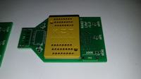
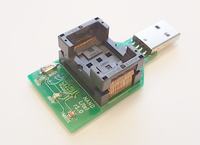
The programmer designed by me, due to the cost cutting, contains only one slot for inserting Flash NAND memory in the TSOP48 housing, soldered permanently.

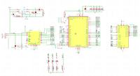
The whole is powered from the USB port with 5.0V voltage, while the FlashNAND memory system and the processor is supplied with 3.3V voltage supplied from the LDO stabilizer TPS781330220. The advantage of this stabilizer is built-in 150mA overcurrent protection, which works great in the case of reverse inserting the system into the stand, which does not damage the memory chip, as well as the fact that I had them in large quantities in the warehouse.
I added two LEDs, indicating the voltage of 5.0V (D5), and 3.3V (D1), after which you can quickly check if everything is in order.
I used a full FlashNAND memory connection system, in which there are four CE lines, and four RB lines, thanks to which it is possible to handle all types of memory available in the TSOP48 enclosure, and the 3.3V power supply is fed only to the VSS pins (13 , 36), VCC (12.37).
The entire programmer is managed by the XMEGA-A4U processor, which perfectly fits in terms of the number of pins with which the software communicates on a PC, through the USB & lt; & gt; FT245.
I used here a very interesting solution based on a parallel bus, connecting the data lines DATA0-7 of the FT245 system directly to the XMEGA processor port, additionally connecting them to the FlashNAND memory system.
I gained a high speed of data transmission and great freedom of communication.
The results I received surprised me:
FT245 & lt; & gt; XMEGA = 980kB / s
NAND & lt; & gt; XMEGA = 2.7MB / s
Thus, the sample communication then looks like:
1. PC - & gt; XMEGA - read command from NAND memory
2. PC & lt; - XMEGA - start reading package
2. XMEGA - & gt; NAND - preparation for reading, sequence execution
3. PC & lt; - NAND - transfer data directly from NAND to PC
4. XMEGA & lt; - NAND - data listening counting CRC32
5. XMEGA - & gt; NAND - end of reading
6. PC & lt; - XMEGA - end of the read packet
In this general procedure, taking into account the protocol overhead and interchangeable communication with the PC, I achieve a real transfer rate of 750kB / s considering the reading time of FlashNAND at 60us.
The programmer also has the ability to measure the time of reading / writing / deleting pages. It performs completely hardware in XMEGA using the Timer with an accuracy of 1us. Due to the fact that the RB outputs of the FlashNAND memory chip are only pulled up by the pull-up resistors in XMEGA, these values differ slightly from those in the documentation. How much, I have to measure it with an oscilloscope. However, it gives us the opportunity to assess the diagnostic of a given FlashNAND memory chip. For example, you can see that some pages are read slightly faster than others. The difference is sometimes significant.
Example: K9GAG08U0E-SCB0
Block 0, page 0: read: 197us
Block 0, page 1: read: 198us
Block 0, page 2: reading: 235us
Block 0, page 3: read: 198us
Block 0, page 4: reading: 236us
Example: MT29F64G08CBAAAWP
Block 0, page 0: reading: 42us
Block 0, page 1: reading: 43us
Block 0, page 2: reading: 42us
Block 0, page 3: reading: 42us
Block 0, page 4: reading: 58us
Block 0, page 5: reading: 58us
Block 0, page 6: reading: 42us
Example: K9F5608U0C-YIB0
Block 0, page 0: read: 9us
Block 0, page 1: read: 9us
Block 0, page 2: reading: 8us
Block 0, page 3: reading: 8us
Block 0, page 4: reading: 8us
Block 0, page 5: reading: 8us
Block 0, page 6: reading: 8us
The programmer also has detection of the system, for this purpose after inserting the system and inserting the programmer into USB the first step is setting the line low / WP to protect the FlashNAND memory system from accidental deletion, waiting 1000ms and after this time the RESET command is sent to the memory then the memory ID is read.
If the loaded identifier has non-different values, eg: 0x00, 0x00, 0x00, then the system is marked as undiscovered and the red LED lights up, and if these values differ from each other, then the green LED lights up. This function has been added to allow you to check whether everything is okay and you can take a PC program right after you insert the system into the stand, or you should improve something in the layout.

Estimated costs about 105 PLN. Assuming that we perform immediately 5 pieces.
The worst is with the TSOP48 socket, which unfortunately has to be imported from China.
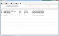
The HEX file of the current version (NANDLite_r1.0_1003a.zip) of the programmer is in the appendix, and the off-line PC application (NANDLite_v1.0.1003.43.zip)
The latest version of the software can be found under the link Link which contains the latest signatures of supported chips.
Cool! Ranking DIY