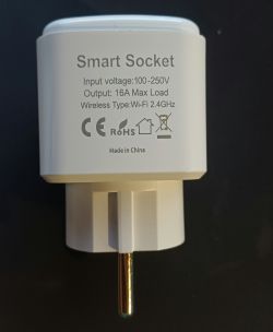
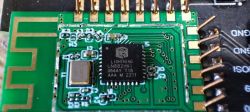
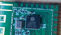
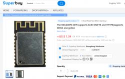
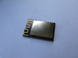
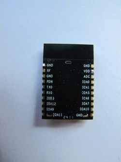
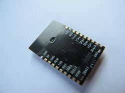
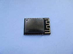
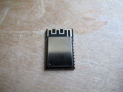
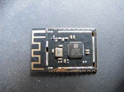
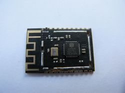
A contact at Lightning Semiconductor, who has been very helpful on Gitee and email, pointed me to this module on Taobao when I asked about getting an LN882H and/or LN8825B development board. LN8825B has been discontinued and is no longer in production and Lightning Semi do not ship dev boards outside of China.
Despite my best efforts I was not able to get a functioning/verified Taobao personal or business account so I could purchase the module for direct shipment to the UK.
Googling around it seemed there were companies that will purchase from such restrictive sites on your behalf then ship them onward to you. Pandabauy.com is one such site. Using the whole Taobao URL in the search field it seemed like it could be a success. Very cheap, but I expected shipping and taxes would be a lot more than the cost of the modules.
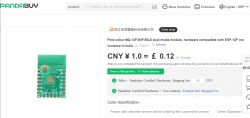
I signed up and purchased 2 modules and a W800 Winner Micro board. First the items will be shipped to the PandaBuy warehouse. When they arrive they are photographed and stored in the warehouse against your account. Photographs are added to your order for inspection.
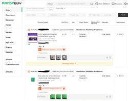
this was the tracking/time taken from order to storage at PandaBuy warehouse
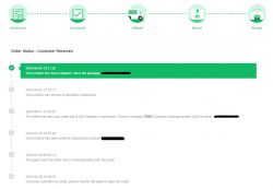
when your items are all received you get to choose an onward postal service. I went with one of the cheapest - China Post/Royal Mail. The expected time to arrival was 2-3 weeks. There was an initial cost but later a partial refund when final weight and parcel dimensions were calculated. In total I think the whole order end to end was ~PLN10 including the W800. The order arrived today, 22nd April, so a total of 3 weeks from first order.

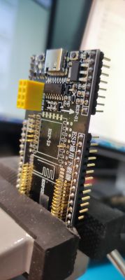
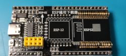
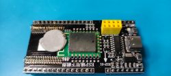
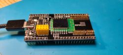
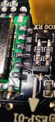
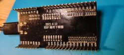
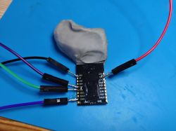
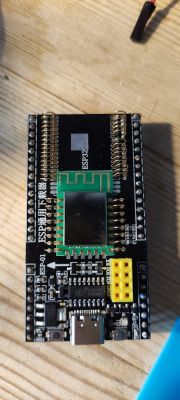
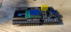
With the modules finally in hand and lifting inspiration from my previous NodeMCU/CB3S transplant and this post here about a universal ESP board, which I got from Ali Express, I fit the module ready for analysis.
Not knowing if the module would come with any development/testing software pre-flashed, I looked out for any new wireless APs broadcasting. Sure enough SSID "MQ_C0DAFA" appeared. On connection my wireless adaptor was DHCP assigned an IP of 192.168.4.2 from server 192.168.4.1, like Tasmota/OpenBeken. Browsing 192.168.4.1 prompts for a username/password. My second guess was admin/admin, which was correct.
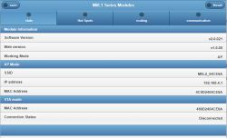
The home page of what comes up
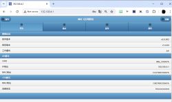
and Chrome translation to English
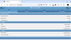
and the remaining main tabs
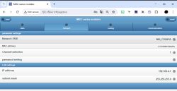
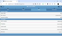
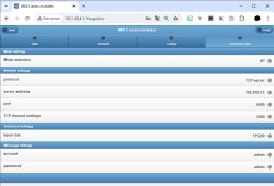
you can drill down further to customise most areas, for example AP/STA/Null wifi mode

On B9/GPIO2 (UART_TX1 pin for log printing, corresponding to pin 30) we get the following (had to use 2000000 baud)
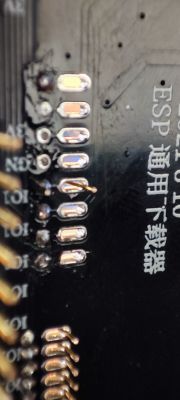
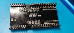
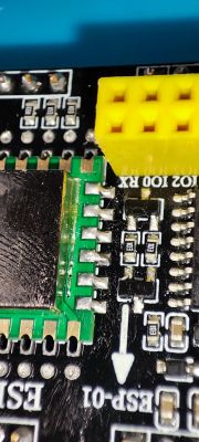
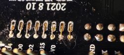
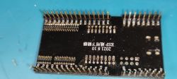
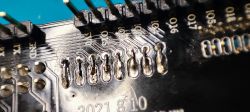
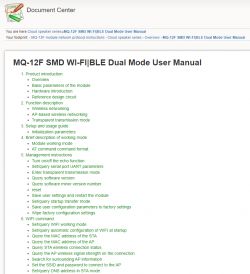
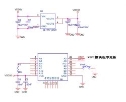
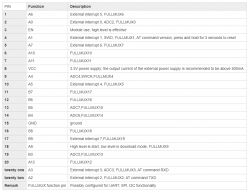
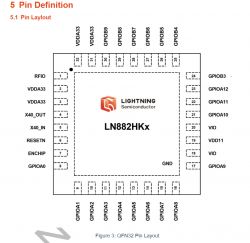
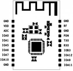
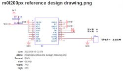
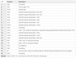
All good stuff, but I want OpenBeken on it. Before erasing and flashing with OBK I want to dump the firmware that it shipped with. The LN modules have their own GPIO/pad name/numbering system so I need to know exactly to which pins on the ESP board each is linked. Using these images as a reference point, and the use of a multi-meter to confirm continuity, we can map the pins.
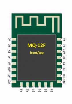
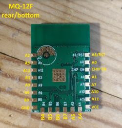
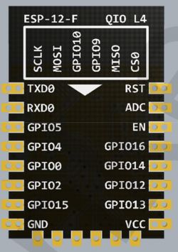
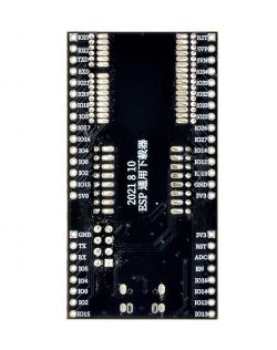
The mappings are:
ESP-12F - MQ-12F
TXD - A2
RXD - A3
GPIO5 - A12
GPIO4 - B3
GPIO0 - A9
GPIO2 - B9
GPIO15 - B8
GND - GND
SCLK - B4
MOSI - B5
GPIO10 - B6
GPIO9 - B7
MISO - A5
CS0 - A4
VCC - VCC
GPIO13 - A11
GPIO12 - A10
GPIO14 - A7
GPIO16 - A1
EN - CHIP EN
ADC - A0
RST - A6/RST
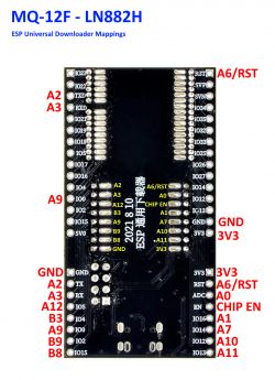
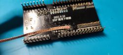
To get LN882H into download mode we need to ground A9 as it's being powered. With the GPIO0/A9 button on the dev board held down as the USB-C cable is inserted, the desired state is obtained. This is the exact method as described in the LN882H flashing guide. It appears you *can* actually release A9 once in download mode. I also achieved the same by bridging GND and GPIO0 pins on the underside of the dev board with a jumper cable.
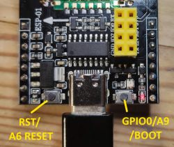
Now the python script can be used with LN882H_CMD_Tool.exe to download the factory firmware. The ESP universal board has a built-in Winchiphead CH340 USB-TTL chip, which for me was COM6, so my command to begin dump was:
This took ~25 mins. I attach the result.
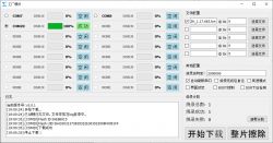
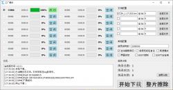
Then, as explained here and in the flashing guide referenced above (for the command line experience), I flashed OBK using the GUI flasher.
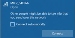
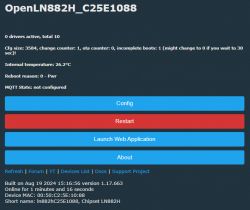
After a reboot, the AP broadcasts as expected

From 192.168.4.1 http you can then join it to your wifi ready for any testing you may wish to do on the LN882H in OpenBeken!
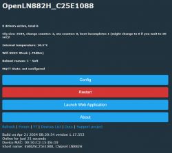
and the LN OBK boot log (921600 baud):
A couple of things of note:
-The factory fw boot log contains the title "at_mqlinks_ln882h" which looks like it might mean it support AT commands. I have not explored this.
-The bottom row of pads on the ESP universal board don't appear to be linked to any pins. I assume the solder pads are there only to hold the module in place.
-The ESP dev board does not have a proper USB-C compliant connector/controller. It is supplying power and standard USB signals, so a USB-C to USB-C cable doesn't work. I used USB-A to USB-C. More on this here.
-Not all same-numbered GPIOs on the ESP board are connected to each other
-The ESP universal downloader board did not ship with pins soldered. These were added by me
Despite my best efforts I was not able to get a functioning/verified Taobao personal or business account so I could purchase the module for direct shipment to the UK.
Googling around it seemed there were companies that will purchase from such restrictive sites on your behalf then ship them onward to you. Pandabauy.com is one such site. Using the whole Taobao URL in the search field it seemed like it could be a success. Very cheap, but I expected shipping and taxes would be a lot more than the cost of the modules.

I signed up and purchased 2 modules and a W800 Winner Micro board. First the items will be shipped to the PandaBuy warehouse. When they arrive they are photographed and stored in the warehouse against your account. Photographs are added to your order for inspection.

this was the tracking/time taken from order to storage at PandaBuy warehouse

when your items are all received you get to choose an onward postal service. I went with one of the cheapest - China Post/Royal Mail. The expected time to arrival was 2-3 weeks. There was an initial cost but later a partial refund when final weight and parcel dimensions were calculated. In total I think the whole order end to end was ~PLN10 including the W800. The order arrived today, 22nd April, so a total of 3 weeks from first order.

With the modules finally in hand and lifting inspiration from my previous NodeMCU/CB3S transplant and this post here about a universal ESP board, which I got from Ali Express, I fit the module ready for analysis.


Not knowing if the module would come with any development/testing software pre-flashed, I looked out for any new wireless APs broadcasting. Sure enough SSID "MQ_C0DAFA" appeared. On connection my wireless adaptor was DHCP assigned an IP of 192.168.4.2 from server 192.168.4.1, like Tasmota/OpenBeken. Browsing 192.168.4.1 prompts for a username/password. My second guess was admin/admin, which was correct.
The home page of what comes up

and Chrome translation to English

and the remaining main tabs


you can drill down further to customise most areas, for example AP/STA/Null wifi mode

On B9/GPIO2 (UART_TX1 pin for log printing, corresponding to pin 30) we get the following (had to use 2000000 baud)
Code: Text
All good stuff, but I want OpenBeken on it. Before erasing and flashing with OBK I want to dump the firmware that it shipped with. The LN modules have their own GPIO/pad name/numbering system so I need to know exactly to which pins on the ESP board each is linked. Using these images as a reference point, and the use of a multi-meter to confirm continuity, we can map the pins.


The mappings are:
ESP-12F - MQ-12F
TXD - A2
RXD - A3
GPIO5 - A12
GPIO4 - B3
GPIO0 - A9
GPIO2 - B9
GPIO15 - B8
GND - GND
SCLK - B4
MOSI - B5
GPIO10 - B6
GPIO9 - B7
MISO - A5
CS0 - A4
VCC - VCC
GPIO13 - A11
GPIO12 - A10
GPIO14 - A7
GPIO16 - A1
EN - CHIP EN
ADC - A0
RST - A6/RST

To get LN882H into download mode we need to ground A9 as it's being powered. With the GPIO0/A9 button on the dev board held down as the USB-C cable is inserted, the desired state is obtained. This is the exact method as described in the LN882H flashing guide. It appears you *can* actually release A9 once in download mode. I also achieved the same by bridging GND and GPIO0 pins on the underside of the dev board with a jumper cable.

Now the python script can be used with LN882H_CMD_Tool.exe to download the factory firmware. The ESP universal board has a built-in Winchiphead CH340 USB-TTL chip, which for me was COM6, so my command to begin dump was:
Code: Text
This took ~25 mins. I attach the result.
Then, as explained here and in the flashing guide referenced above (for the command line experience), I flashed OBK using the GUI flasher.

After a reboot, the AP broadcasts as expected
From 192.168.4.1 http you can then join it to your wifi ready for any testing you may wish to do on the LN882H in OpenBeken!

and the LN OBK boot log (921600 baud):
Code: Text
A couple of things of note:
-The factory fw boot log contains the title "at_mqlinks_ln882h" which looks like it might mean it support AT commands. I have not explored this.
-The bottom row of pads on the ESP universal board don't appear to be linked to any pins. I assume the solder pads are there only to hold the module in place.
-The ESP dev board does not have a proper USB-C compliant connector/controller. It is supplying power and standard USB signals, so a USB-C to USB-C cable doesn't work. I used USB-A to USB-C. More on this here.
-Not all same-numbered GPIOs on the ESP board are connected to each other
-The ESP universal downloader board did not ship with pins soldered. These were added by me
Cool? Ranking DIY


