
logo elektroda
logo elektroda
X
logo elektroda

[Youtube] How to make BK7231 development board - NodeMCU conversion - soldering guide, hot air, SMD

p.kaczmarek2 7530 37

TL;DR LABEL_AI_GENERATED

  • A cheap NodeMCU ESP8266 board is converted into a BK7231 development board by transplanting a CB3S or WB3S Wi‑Fi module.
  • The process desolders the ESP12 with a hot air station, then solders the BK7231 module in its place using flux, leaded solder, solder wick, and PCB cleaner.
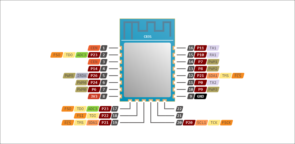
  • CB3S and WB3S are both covered, and CB3S has a slightly different pinout than WB3S.
  • The guide includes basic soldering tips, new pin mappings, and a working development-board demonstration.
AI summary based on the discussion. May contain errors.
ADVERTISEMENT
Listen:
  • [Youtube] How to make BK7231 development board - NodeMCU conversion - soldering guide, hot air, SMD
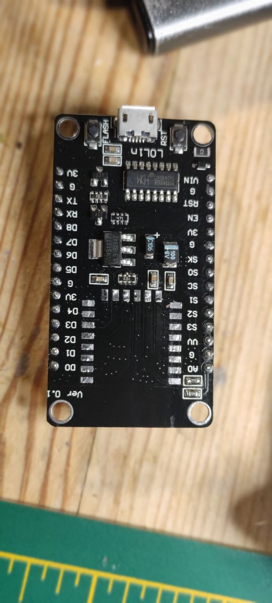
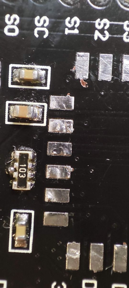
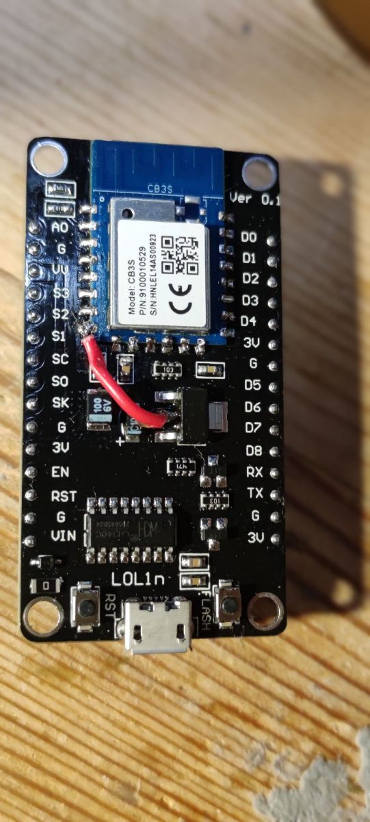
    Here's a step by step guide showing how to make a BK7231 development board (WB3S and CB3S versions) from a very cheap NodeMCU ESP8266 board, by doing a simple WiFi module transplant. First we desolder ESP12 module with a hot air station, and then we solder a CB3S (or WB3S) in it's place. Our guide includes some basic soldering tips, so even a beginner should be able to do the shown process.

    We are aware that there is already some kind of BK7231 development board that can be bought online, but our solution is cheaper and more general. Futhermore, many people already might have a BK7231 module desoldered from IoT device (or may use this opportunity to do a WiFi module swap between NodeMCU and IoT device).

    What is required for this project?
    - CB3S or WB3S module (you can get that from IoT device, and solder the ESP from the NodeMCU in place)
    - hot air station (cheapest one will be enough)
    - basic soldering equipment and soldering iron will be also needed, so flux, leaded (Pb) solder, solder wick, PCB cleaner
    - NodeMCU board (it can be bought very cheaply online, it's available in many shops)

    Here's the guide:
    [youtube]
    https://www.youtube.com/watch?v=xGE-DVrm3BU
    [/youtube]
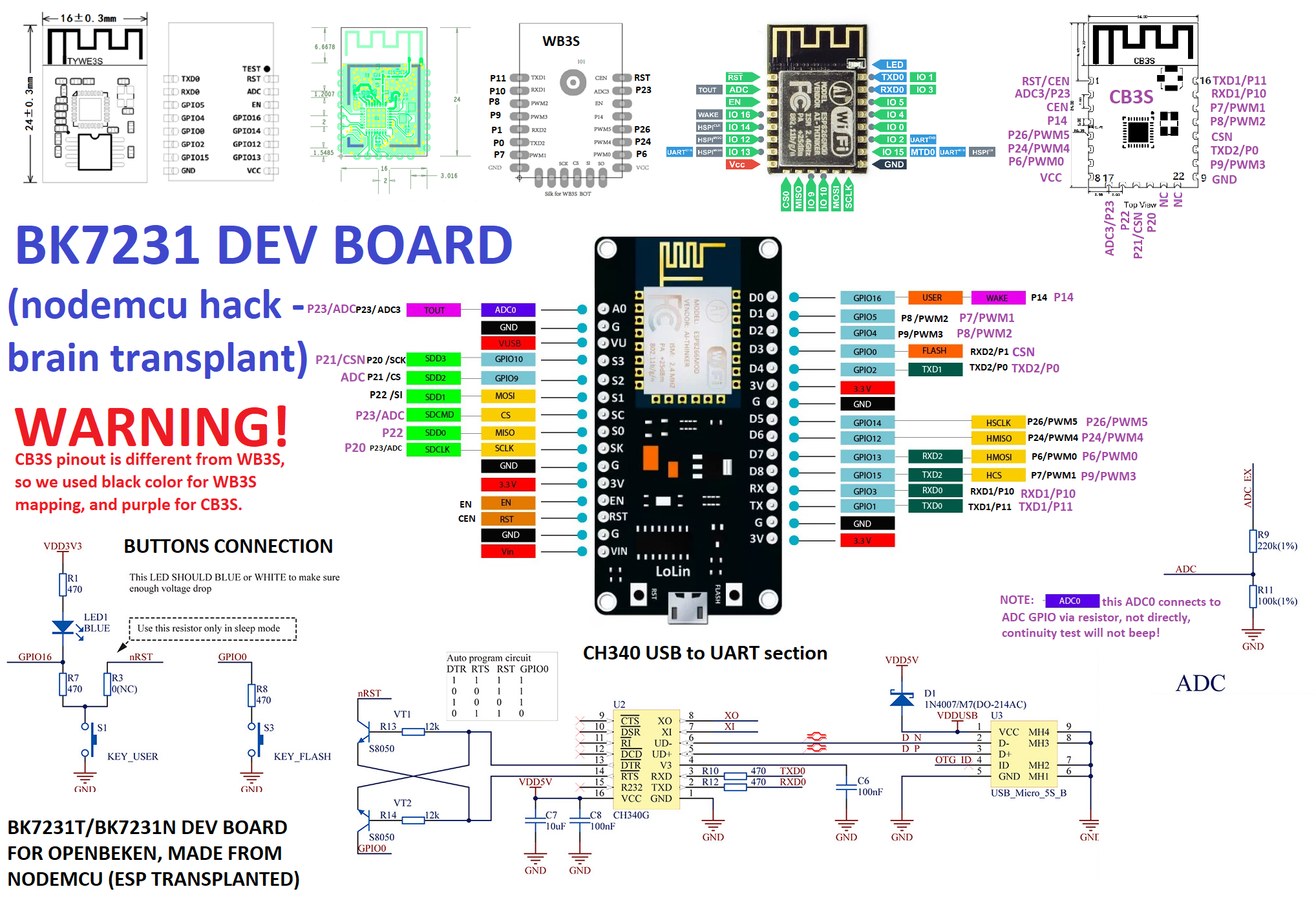
    In addition, we're including a new pin mappings for a BK7231 board created that way.
    Warning: CB3S has slightly different pinout than WB3S, both pinout versions are included on the guide below:
    [Youtube] How to make BK7231 development board - NodeMCU conversion - soldering guide, hot air, SMD
    Here is NodeMCU schematic:
    [Youtube] How to make BK7231 development board - NodeMCU conversion - soldering guide, hot air, SMD
    Dev board in action:
    [Youtube] How to make BK7231 development board - NodeMCU conversion - soldering guide, hot air, SMD
    [Youtube] How to make BK7231 development board - NodeMCU conversion - soldering guide, hot air, SMD

    Thank you for watching. Please consider giving us a like and/or subscribe.
    You can also visit out BK7231 firmware page:
    https://github.com/openshwprojects/OpenBK7231T_App
    our BK7231 flash tool:
    https://github.com/openshwprojects/BK7231GUIFlashTool
    and our IoT devices teardowns list:
    https://openbekeniot.github.io/webapp/devicesList.html

    Have fun tinkering and stay free from the cloud!

    Cool? Ranking DIY
    Helpful post? Buy me a coffee.
    About Author
    p.kaczmarek2
    Moderator Smart Home
    Offline 
    p.kaczmarek2 wrote 14755 posts with rating 12881, helped 659 times. Been with us since 2014 year.
  • ADVERTISEMENT
  • #2 20550752
    Anonymous
    Level 1  
  • ADVERTISEMENT
  • BK7231 board avoids hot-air desoldering of ESP module

    #3 20550797
    p.kaczmarek2
    Moderator Smart Home
    Posts: 14755
    Help: 659
    Rate: 12881
    Great idea! I was not aware that there is a relatively cheap board for this pad format and without a soldered module, although in retrospect it seems obvious.

    However, I would not be afraid of the "destruction" itself, because the ESP can go to the place of the desoldered WB3S / CB3S and there is a wolf full and a whole sheep, while the @khoam solution has another great advantage - no need to desolder with hot air ESP.
    Helpful post? Buy me a coffee.
  • ADVERTISEMENT
  • #5 20553519
    p.kaczmarek2
    Moderator Smart Home
    Posts: 14755
    Help: 659
    Rate: 12881
    Good job with conversion. Which soldering station did you use?

    Btw, from a brief glance, it looks like the TM1638 on your photo may be very similar to gn6932 and also to TM1637. We'll see how it goes.
    Helpful post? Buy me a coffee.
  • #6 20555441
    DeDaMrAz
    Level 23  
    Posts: 620
    Help: 34
    Rate: 130
    From 1.17.53 build, you can switch logging UART via the example below:

    // Enable "[UART] Enable UART command line"
    // this also can be done in flags, enable command line on UART1 at 115200 baud
    SetFlag 31 1
    // UART1 is RXD1/TXD1 which is used for programming and for TuyaMCU/BL0942,
    // but now we will set that UART1 is used for log
    logPort 1
  • #7 20555512
    p.kaczmarek2
    Moderator Smart Home
    Posts: 14755
    Help: 659
    Rate: 12881
    Yes, setting UART1 as log port (instead of UART2) will help on this board a lot, because UART1 has the CH340 hooked up (and is also used for programming), while, on the other hand, the default UART2 would require user to connect separate UART to USB converter, just to get log.
    Helpful post? Buy me a coffee.
  • ADVERTISEMENT
  • Helpful post

    CB3S removed cleanly with flux and braid

    #9 21012724
    divadiow
    Level 38  
    Posts: 5213
    Help: 446
    Rate: 914
    my work in progress

    Three electronic devices on a green cutting mat.

    I've butchered this device for its CB3S https://www.elektroda.com/rtvforum/topic4027954.html#20904497

    I kind of hate the battery powered deep sleep devices, so it's no loss. I'd hope to solder the ESP onto it though to see what Tasmota is like on battery.

    Not many of the CB3S pins were soldered so this was relatively easy with some extra pb solder, flux and braid. I was switching from side to side quite quickly but also inching it upwards from the top. Luckily I did not break any pads.

    I don't have a heat gun, so the NodeMCU is going to be a challenge. All pins on all sides are soldered 🥵
  • #10 21012728
    p.kaczmarek2
    Moderator Smart Home
    Posts: 14755
    Help: 659
    Rate: 12881
    Heat gun is there a must have. Maybe you could try to use a high power soldering iron and form a U shape with a thick wire that will heat all pads at once but I am not sure if it will have enough heating capacity for it.
    Helpful post? Buy me a coffee.
  • #11 21012740
    divadiow
    Level 38  
    Posts: 5213
    Help: 446
    Rate: 914
    Very interesting idea! Or I have two soldering irons, one is old and in my recycling bag, but it could be brought back to life for some double-iron multi sided action.

    Added after 8 [hours] 11 [minutes]:

    >>20550752
    Oh! Or get this. Not as much fun though
  • Bodged 3.3V pad after trace damage

    #12 21020097
    divadiow
    Level 38  
    Posts: 5213
    Help: 446
    Rate: 914
    It didn't go too badly. Fairly smooth until the very end. The bent soldering iron to cover two corners wasn't a success - the original tip was too fat and the bend too curved to be effective. Nails and other thinner tips tried wouldn't get hot enough to melt the solder. Success was with holding the old soldering iron along the short bottom edge and using the quick-move trick on the other two sides, each with long pb solder sausage covering pins.

    Two soldering irons on a work mat next to a small electronic module.
    The hooked solder was pulling the module forward so when it finally freed it shot across the desk.

    These were pads before cleanup after module came off
    PCB mounted in a holder on a workshop desk.

    Then clean-up. Yes, I damaged the trace of 3V while braiding! 😭

    Electronic module with multiple connectors on a wooden desk.
    Close-up of a printed circuit board with soldered SMD components and copper traces.

    The copper only looked exposed so I proceeded to align and solder a corner of the CB3S module. Yes, I should have checked continuity to 3.3v.

    Close-up of an electronic module CB3S with visible markings and soldered pins.

    then other pads
    Close-up of a CB3S module on a circuit board with visible solder pins.

    Unfortunately that 3.3V pad was more damaged than I thought, there was no continuity between the AMS117 and of course the module was not powering. I wasn't in the mood to desolder to investigate, so here's a working bodge

    Close-up of a circuit board with a red wire soldered to electronic components. CB3S electronic module board with components and connections.

    80% happy with it. I just need to test GPIOs next. It came up with the OBK config of previous device but when flashed to latest OBK using OTA it did not reappear. I reflashed erased/redid RF partition but ultimately ended up going back to the original device fw then OBK again. No problem, I guess something was a little unhappy with all the changes. It's nice to have a BK board with soldered RST button and USB-TTL in such close proximity - Easy Flasher connected at max baud and flashed very quickly. Good to know a hot air gun isn't the only option to remove 3-sided modules.

    OpenBK_BK7231N_CB3S_NodeMCU interface screen with configuration options.

    autoexec is as above

    Code: Text
    Log in, to see the code
  • Standard GPIOs work; one LED is dimmer

    #13 21025311
    divadiow
    Level 38  
    Posts: 5213
    Help: 446
    Rate: 914
    decent outcome. all of the normal/standard GPIOs work fine. assume a couple are default pull-high because the LEDs come on as soon as the board is powered. one LED is duller than the rest - S3/P20/SCK - I'm guessing it has a (different?) internal resistor to the others, or just has one. I can't find the right bit in a datasheet yet.

    Breadboard with LEDs in various colors next to a microcontroller connected by wires.

    Screenshot of OpenBK user interface with toggles and system information.
  • #14 21025386
    p.kaczmarek2
    Moderator Smart Home
    Posts: 14755
    Help: 659
    Rate: 12881
    That's an interesting finding. I'd first double check, maybe there is an extra resistor on the board or something. Also I'd just swap in place two of the LEDs just to be sure it's not a faulty LED.

    You can drive even more LEDs with OBK if you use ShiftRegister
    Helpful post? Buy me a coffee.
  • #15 21048388
    divadiow
    Level 38  
    Posts: 5213
    Help: 446
    Rate: 914
    >>20550752

    yes. these are cool

    Prototype board with ESP module and connected USB cable.
  • #16 21048393
    p.kaczmarek2
    Moderator Smart Home
    Posts: 14755
    Help: 659
    Rate: 12881
    So, do they work good for BK7231? How do you do power cycle there - CEN?
    Helpful post? Buy me a coffee.
  • Reset button starts Easy Flasher dump on BK board

    #17 21048408
    divadiow
    Level 38  
    Posts: 5213
    Help: 446
    Rate: 914
    i've not got a BK module loose to try, but it has a reset button (bottom right in my pic) the same as other dev boards. I have started flash dump in Easy Flasher using this button. I've only tested RX/TX with this but I see no reason why the other pins won't be fine too.

    Good to know that at least these modules, and probably more, can be used in the ESP-12 half of this one board alone

    BT3L, CB3S, CB3L, CR3L, C-8138, ESP-12, FL_M93_V1, MRE3S, MWA04, MWA6S, T103, TYWE3L, TYWE3S, XR3, WB3, WB3L, WB3N, WB3R, WB3S, WB8, WR3, WR3E, WR3L, WR3N, ZS3L, HLK-B30, ESP32-C3

    I got it for when these LN882H modules arrive https://www.elektroda.com/rtvforum/topic4023264.html#21024176

    Added after 43 [seconds]:

    divadiow wrote:
    i've not got a BK module loose to try


    actually not strictly true. HLK-B30 is Beken 🙄. I don't have a regular BK module like CB3S loose

    Added after 13 [minutes]:

    @p.kaczmarek2 get one or two!
  • P20 maps to SK, not S3 on transplant board

    #18 21065038
    divadiow
    Level 38  
    Posts: 5213
    Help: 446
    Rate: 914
    can someone please check continuity from P20 on the CB3S to S3 on the nodeMCU if they've done the transplant.

    mine maps to SK pin not S3 as shown on the diagram in first post

    Fragment of a circuit diagram showing pin assignments for CB3S and NodeMCU.

    Diagram of the CB3S module with labeled pins and their functions.

    also P21 goes to S3. I am detecting an I2C device successfully using S3 and SK.

    Screenshot showing pin settings for P20 and P21 for SoftSCL and SoftSDA.

    Info:I2C:Address 0x77 (dec 119)
  • #20 21065056
    divadiow
    Level 38  
    Posts: 5213
    Help: 446
    Rate: 914
    thanks!

    grr

    wish I'd double-checked diagram was correct ages ago.
  • #21 21065609
    p.kaczmarek2
    Moderator Smart Home
    Posts: 14755
    Help: 659
    Rate: 12881
    Ah, so there was a mistake in the diagram? I will update it in a moment. This may explain why your BMP280 was not working (or which chip was it?), @divadiow
    Helpful post? Buy me a coffee.
  • #22 21065620
    divadiow
    Level 38  
    Posts: 5213
    Help: 446
    Rate: 914
    p.kaczmarek2 wrote:
    This may explain why your BMP280 was not working (or which chip was it?)


    BMP280/AHT20, yes. But I did try SDA2 on BK and was getting i2c address return. I have since tested with S3/SK and still the same. My BMP280 (no AHT) should arrive this afternoon so I'll know for sure.

    Added after 37 [seconds]:

    I was also trying with BL602 PR with BMP280 driver
  • #23 21065688
    p.kaczmarek2
    Moderator Smart Home
    Posts: 14755
    Help: 659
    Rate: 12881
    Ok, can you check, is this diagram better?
    BK7231 Dev Board schematic with connections and warnings.
    Helpful post? Buy me a coffee.
  • #24 21065795
    divadiow
    Level 38  
    Posts: 5213
    Help: 446
    Rate: 914
    hmmm. I think this is closer

    BK7231 development board schematic with pinouts and connections.
  • #25 21065822
    p.kaczmarek2
    Moderator Smart Home
    Posts: 14755
    Help: 659
    Rate: 12881
    So S0 is not connected?
    Helpful post? Buy me a coffee.
  • #26 21065832
    divadiow
    Level 38  
    Posts: 5213
    Help: 446
    Rate: 914
    oh no. I've fallen victim to reversed and non-reversed references. ignore me. I'll check again

    Added after 9 [minutes]:

    OK.

    Diagram of BK7231 development board with pin descriptions and detailed connection schematics.
  • CEN button as power-cycle workaround

    #27 21075406
    divadiow
    Level 38  
    Posts: 5213
    Help: 446
    Rate: 914
    that last image is good/final I believe?

    Added after 16 [minutes]:

    p.kaczmarek2 wrote:
    So, do they work good for BK7231? How do you do power cycle there - CEN?


    yes, this is an issue for me with MQ-12F. I've been unplugging board to power off but I guess CEN is an option. maybe some extra push button to ground cen could be fit in somewhere

    the other drawback of those ESP universal boards of course is the bottom row of pads don't trace anywhere.

    These are perhaps a nicer option. they seem sturdier anyway. I haven't used this one yet
    ESP8266 development board on a blue surface next to a plastic box labeled ESP8266.

    Added after 6 [minutes]:

    https://www.aliexpress.com/item/1005005850152605.html
  • #28 21342107
    p.kaczmarek2
    Moderator Smart Home
    Posts: 14755
    Help: 659
    Rate: 12881
    I have split BK7238 discussion to:
    NiceMCU XH-WB3S Flashing, testing, pinout, development
    Helpful post? Buy me a coffee.
  • #29 21360877
    p.kaczmarek2
    Moderator Smart Home
    Posts: 14755
    Help: 659
    Rate: 12881
    Today my WEMOS W1F1 D1 (with ESP8266 module) arrived (along with BK7238 NiceMCU).
    NiceMCU module with BK7238, WEMOS W1F1 D1, pinheader on a wood surface.
    I wonder if it would make sense to convert D1 to BK7231? Then we could test Arduino shields with it...
    Helpful post? Buy me a coffee.
  • #30 21360932
    divadiow
    Level 38  
    Posts: 5213
    Help: 446
    Rate: 914
    I don't even know what Arduino Shields are. Googling time!
Listen:

Topic summary

LABEL_AI_GENERATED
The discussion centers on converting a cheap NodeMCU ESP8266 development board into a BK7231 development board by transplanting a BK7231 WiFi module (CB3S or WB3S) onto the NodeMCU PCB after desoldering the original ESP12 module using a hot air station. This method offers a cost-effective and flexible alternative to buying dedicated BK7231 dev boards, especially for users who have BK7231 modules salvaged from IoT devices. Key tools include a hot air station and basic soldering equipment, with some users exploring alternative heating methods like dual soldering irons due to lack of a heat gun. The transplant process involves careful desoldering, pad cleanup, and pin mapping verification, with some discussion on correcting pinout diagrams for I2C lines (S3, SK, SC) to ensure sensor compatibility (e.g., BMP280, AHT20). UART logging configuration is also addressed, recommending UART1 for logging due to CH340 USB interface connection. Additional topics include testing of TM1638 displays, power cycling via CEN or reset buttons, and the use of ShiftRegister for driving more LEDs. The community also explores software tools for pin mapping visualization and integration with OpenBK firmware. Alternative inexpensive boards without pre-soldered ESP modules are noted as options to avoid destructive desoldering. The conversation extends to related modules and development boards such as BK7238 NiceMCU, WEMOS W1F1 D1, and various BK series modules (CB2S, WB2S, CB3L, etc.), with interest in Arduino shield compatibility and custom firmware adaptations.
AI summary based on the discussion. May contain errors.

FAQ LABEL_AI_GENERATED

TL;DR: In 3 main steps, a cheap NodeMCU ESP8266 can become a BK7231 dev board; the expert warning is "no need to desolder with hot air" if you choose a blank ESP-12 adapter instead. This FAQ helps OpenBeken users build, wire, flash, and debug CB3S/WB3S boards. [#20550797] Why it matters: This conversion gives BK7231 tinkerers a USB-TTL-equipped development board while reusing common ESP8266 hardware.

Option Best use Main advantage Main drawback
NodeMCU ESP8266 transplant Reusing a spare NodeMCU CH340 USB-TTL, reset button, 3.3 V rail Requires ESP-12 removal
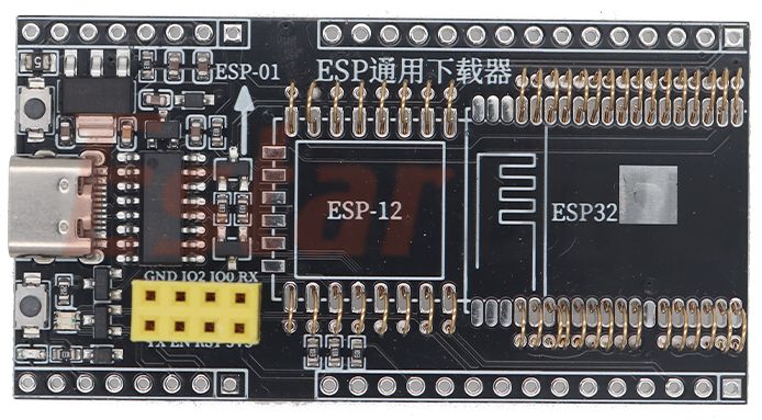
Blank ESP-12 adapter board New BK7231 dev build No ESP desoldering needed Some bottom pads may not route anywhere
Universal ESP module board Testing many module footprints Supports CB3S, WB3S, ESP-12, ESP32-C3, HLK-B30 and more CEN/reset handling may need extra attention

Key insight: The transplant works, but pin mapping matters more than the soldering once the module boots. Always verify continuity before trusting a diagram, especially around S3, SC, SK, P20, P21, and P23.

Quick Facts

  • Required parts are a CB3S or WB3S module, a NodeMCU board, hot air, flux, Pb solder, solder wick, PCB cleaner, and a soldering iron. [#20549683]
  • OpenBeken build 1.17.53 can move logging to UART1 using SetFlag 31 1 and logPort 1. [#20555441]
  • UART1 on this converted board uses RXD1/TXD1, programming pins, CH340 USB-TTL, and a default speed of 115200 baud. [#20555516]
  • Confirmed CB3S mappings include S3 → P21, SC → P23, and SK → P20 after continuity checks. [#21065051]
  • A universal ESP adapter was reported to support over 25 module names, including BT3L, CB3S, WB3S, ESP-12, HLK-B30, and ESP32-C3. [#21048408]

How do you convert a cheap NodeMCU ESP8266 board into a BK7231 development board using a CB3S or WB3S module?

Remove the ESP-12 module and solder a CB3S or WB3S module in its place.
  1. Heat and desolder the ESP-12 from the NodeMCU.
  2. Clean pads with flux, Pb solder, wick, and PCB cleaner.
  3. Align the CB3S or WB3S, tack one corner, then solder all pads.
The original guide shows both CB3S and WB3S versions, plus a working board after conversion. [#20549683]

What tools and soldering supplies are needed to transplant a BK7231 CB3S or WB3S module onto a NodeMCU board?

You need a CB3S or WB3S module, NodeMCU board, hot air station, soldering iron, flux, Pb solder, solder wick, and PCB cleaner. The thread says even the cheapest hot air station is enough for the job. The module can come from a Tuya-style IoT device, while the removed ESP can go back into that donor device. [#20549683]

What is the difference between CB3S and WB3S pinouts when converting a NodeMCU board to BK7231?

CB3S and WB3S use slightly different pinouts, so you must use the correct mapping image before soldering. The first post explicitly warns that CB3S has a different pinout than WB3S. Later continuity checks corrected specific CB3S NodeMCU labels, including S3, SC, SK, P20, P21, and P23. [#20549683]

NodeMCU conversion vs blank ESP-12 adapter board: which is better for making a BK7231 dev board?

Use NodeMCU when you want built-in CH340 USB-TTL and reset hardware; use a blank ESP-12 adapter when you want less desoldering. One participant noted that inexpensive boards exist with everything except the ESP module. The original author agreed their key benefit is "no need to desolder with hot air" from a NodeMCU. [#20550797]

How can you remove an ESP-12 module from a NodeMCU board without a hot air station?

You can remove it with soldering irons and extra Pb solder, but the thread treats this as a harder workaround. One successful method heated the short bottom edge with an old iron, then used long Pb solder across the other two sides. The failure risk is real: the module shot across the desk, and a 3.3 V trace was damaged during cleanup. [#21020097]

What soldering station or hot air station works well for desoldering ESP-12, CB3S, or WB3S modules?

A basic hot air station works; the guide says the cheapest one is enough. A later comment calls a heat gun a must-have for clean ESP-12 removal from NodeMCU. Without hot air, high-power soldering iron tricks may work, but they need enough heat capacity for three soldered module edges. [#21012728]

How do you fix a damaged 3.3V pad or trace after removing the ESP8266 module from a NodeMCU board?

Bridge the damaged 3.3 V path with a bodge wire after confirming lost continuity. One build lost continuity between the AMS1117 regulator and the module after pad cleanup. The board did not power the CB3S until a direct repair wire restored the 3.3 V connection. Always check continuity before final soldering. [#21020097]

How do you configure OpenBeken to use UART1 for logging on a converted BK7231 NodeMCU board?

Enable the UART command line and set UART1 as the log port. Use this OpenBeken script: SetFlag 31 1 logPort 1 This works from build 1.17.53. The thread notes UART1 uses RXD1/TXD1, which are also used for programming and TuyaMCU or BL0942 connections. [#20555441]

What is UART, and why does switching the OpenBeken log port from UART2 to UART1 help on a NodeMCU-based BK7231 board?

UART1 helps because the NodeMCU board already connects it to the CH340 USB-TTL chip. "UART is a serial communication interface that sends and receives data over TX and RX pins, commonly used for logs, command lines, firmware flashing, and module-to-host debugging at fixed baud rates." The default UART2 would need a separate USB-to-UART converter just for logs. [#20555512]

What is CEN on BK7231 modules, and how can it be used for reset or power-cycle behavior on ESP adapter boards?

CEN is the reset-enable control line used to restart BK modules on adapter boards. "CEN is a BK module control pin that resets or enables the chip, letting a button or ground connection restart the module without fully unplugging the USB-powered adapter." One adapter had a reset button, and another user considered adding a push button to ground CEN. [#21075406]

What is a ShiftRegister in OpenBeken, and how can it help drive more LEDs from a BK7231 board?

ShiftRegister lets OpenBeken drive more LEDs than the directly available GPIO pins. "ShiftRegister is an OpenBeken driver feature that expands digital outputs through an external serial register, allowing one BK7231 board to control multiple LEDs using fewer native GPIO pins." It was suggested after testing normal GPIO-driven LEDs on the converted board. [#21025386]

What are the correct CB3S-to-NodeMCU pin mappings for S3, SC, SK, P20, P21, and P23 after the transplant?

The verified mapping is S3 → P21, SC → P23, and SK → P20. This corrected an earlier diagram error. The mistake affected I2C testing because the user expected P20 to map to S3, but continuity showed P20 went to SK. P21 went to S3 instead. [#21065051]

Why might an I2C BMP280 or AHT20 sensor be detected but not work correctly on a converted BK7231 NodeMCU board?

Wrong pin mapping can make I2C appear partly alive while the sensor still fails. The thread found an I2C device at address 0x77, but later discovered the NodeMCU diagram mixed S3 and SK-related mappings. The affected test involved BMP280/AHT20 modules and OpenBeken I2C pins. [#21065038]

What are Arduino shields, and why would converting a WEMOS W1F1 D1 ESP8266 board to BK7231 be useful for testing them?

Arduino shields are plug-in add-on boards for the Arduino-style header layout. "Arduino shields are expansion boards that stack onto compatible development boards, adding hardware such as displays, relays, sensors, or interfaces through predefined header positions." A converted WEMOS W1F1 D1 could let BK7231 firmware test those shield-style peripherals. [#21361714]

How could OpenBeken display NodeMCU-style pin names alongside classic BK7231 GPIO names to avoid wiring mistakes?

OpenBeken could load a board map and show NodeMCU labels beside BK GPIO names in the pins UI. The thread proposed a boards.json approach, mouse-hover highlighting, and integration with the pins chooser and GPIO doctor. The goal was to reduce daily lookup errors between NodeMCU labels and classic BK7231 names. [#21362780]
AI summary based on the discussion. May contain errors.
ADVERTISEMENT