 .
.
In 2021, I featured two switches in the QTouch series on the forum, both of which were based on the ESP8285. Today I'm going back and checking out the latest copies in the same series, has anything inside changed in four years? And if so, how can they now be freed from the cloud and paired with Home Assistant? Let's find out!
The 'single' version can be bought for as little as PLN43, while the 'double' version can be bought for PLN55. I'll cover both versions here, but first I recommend the older 2021 themes:
QTouch WiFi switch plugged into L-wire only - test, interior, schematic .
Smart QTouch WiFi dimmer light switch [Schematic, UART protocol] .
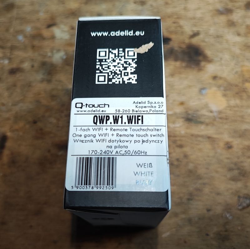
And now it's time to unpack the purchases.... The "single" version first:
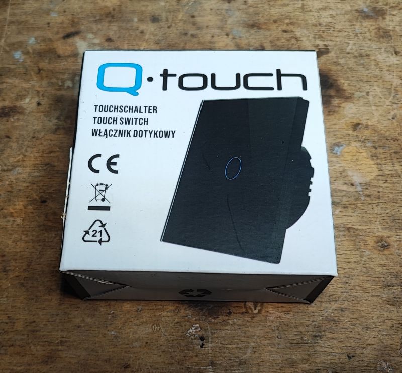
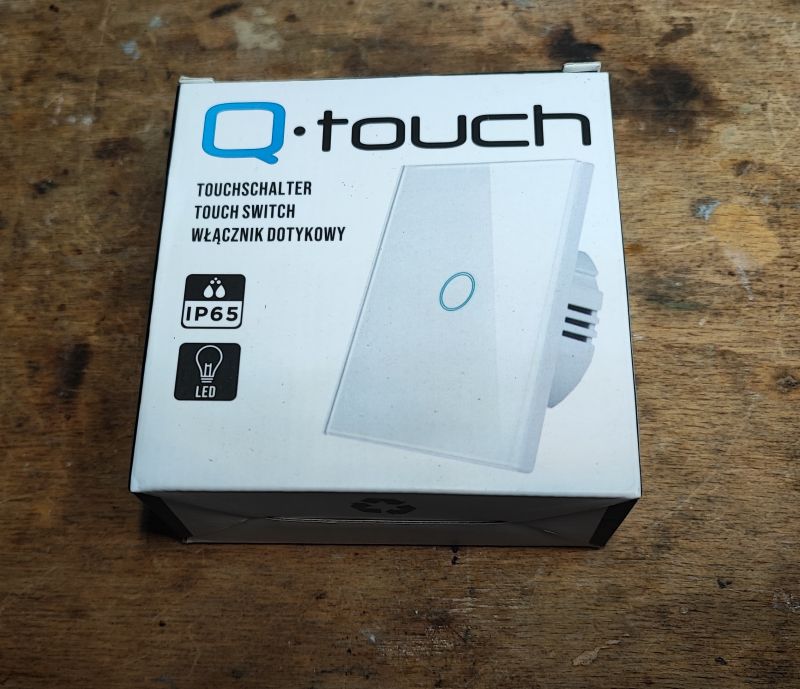
 .
.
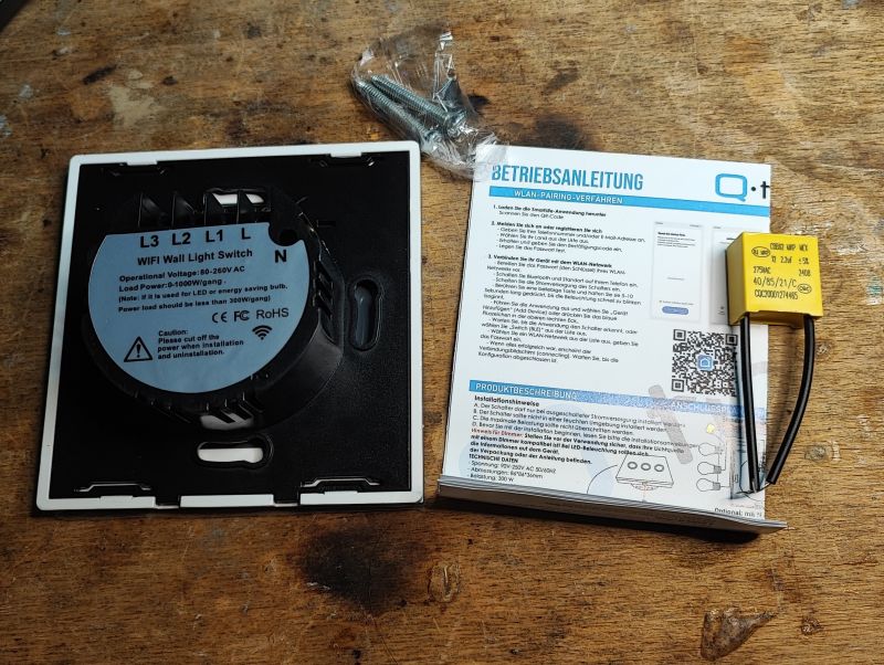
QWP.W1.WiFi, there is a capacitor included, also referred to as an "adapter" by retailers:
 .
.
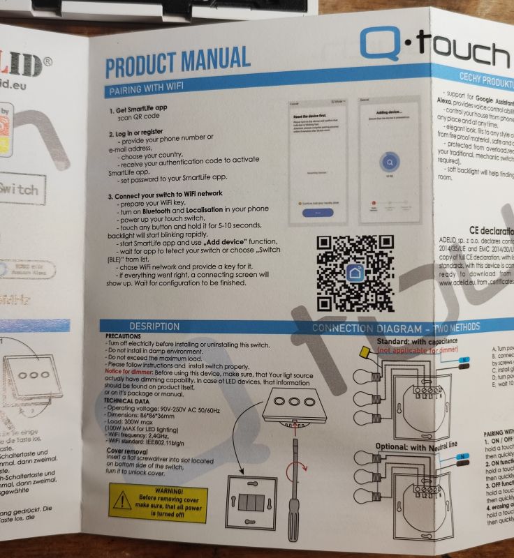
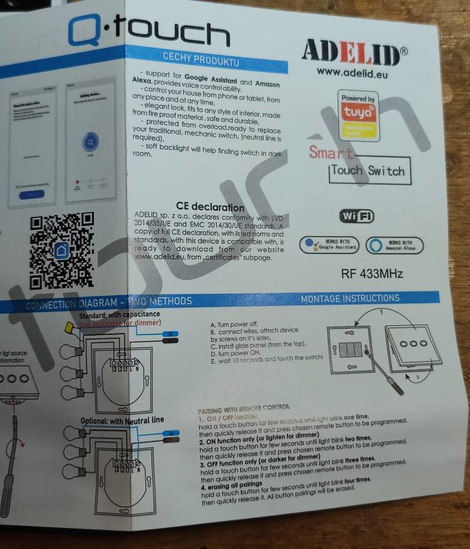
Instructions:
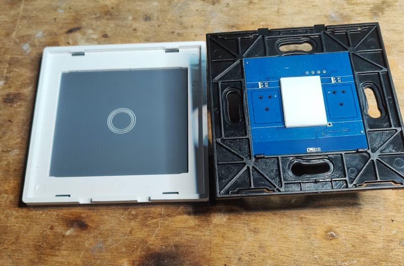
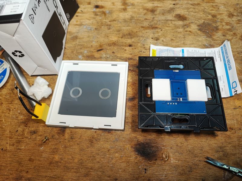
Removed front:
 .
.
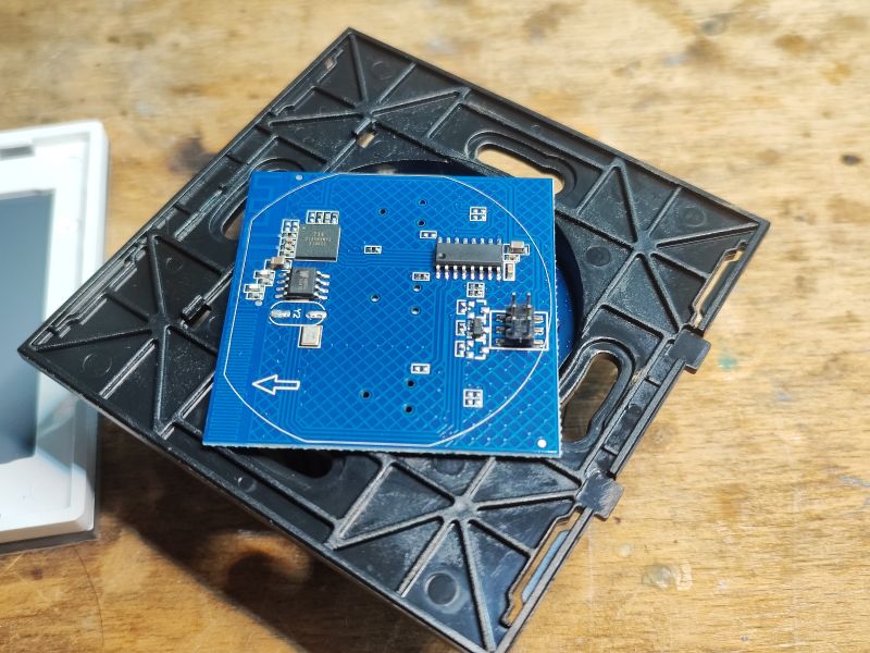
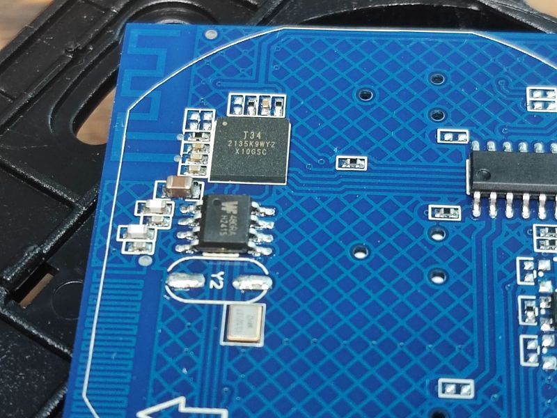
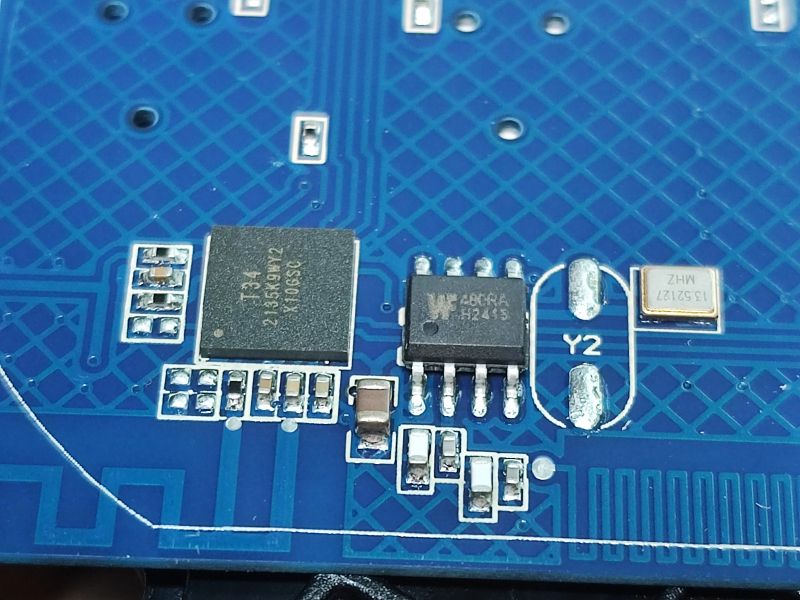
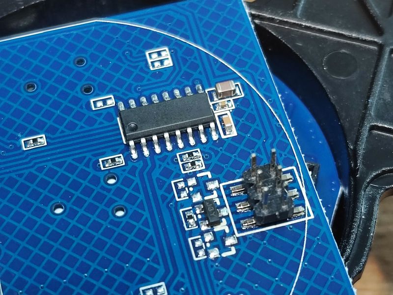
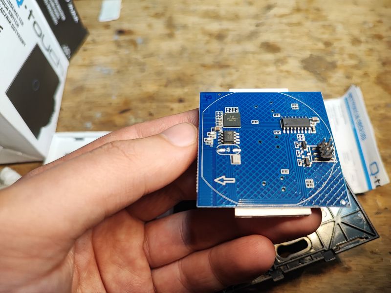
And here is the interior:
 .
.
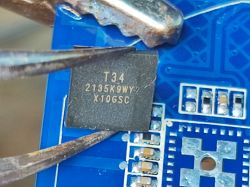
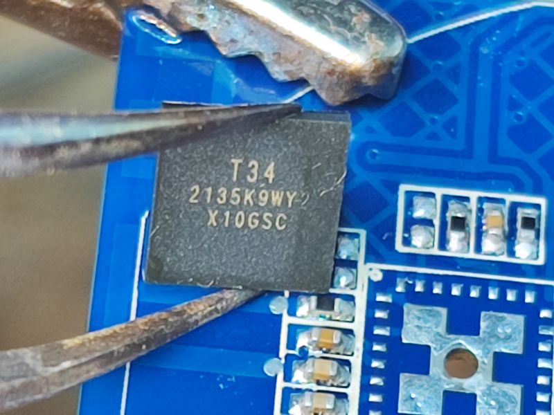
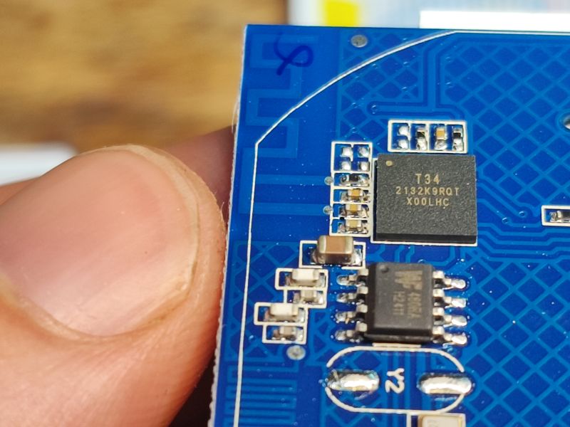
There is a T34 inside, which is essentially a BK7321. You can't upload Tasmota, but you can upload OpenBeken:
https://github.com/openshwprojects/OpenBK7231T_App
https://github.com/openshwprojects/BK7231GUIFlashTool
For RF we additionally have a 480RA chip here, and the third chip in the SOIC housing is the touch button controller.
The RF chip is connected to it, so after changing the RF firmware it will continue to work.
We still have a separate 'executive' board with a rather interesting circuit that I have not analysed:
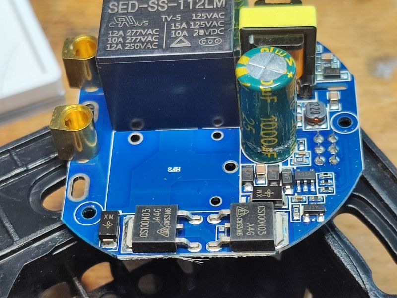
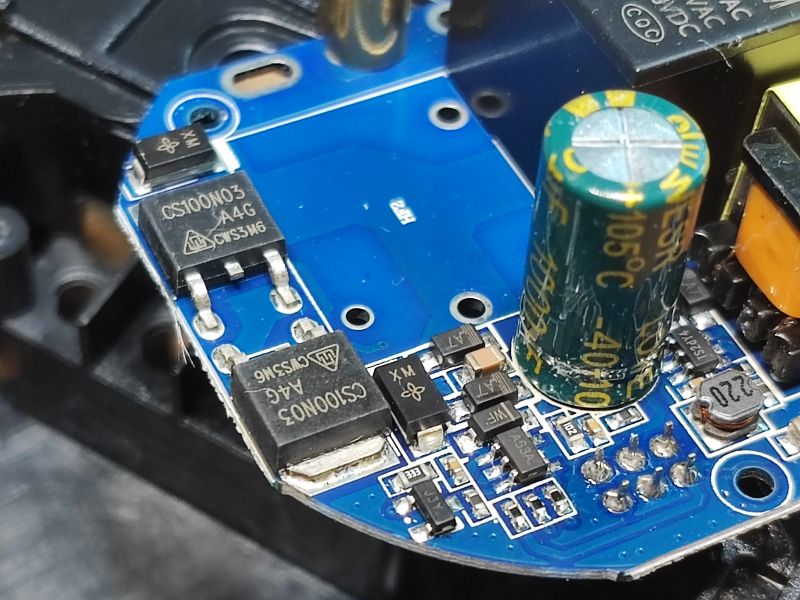
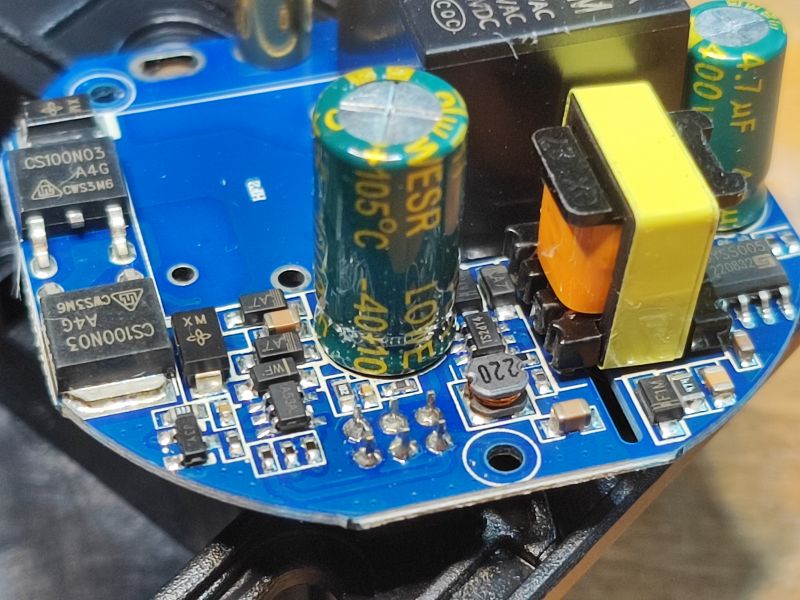
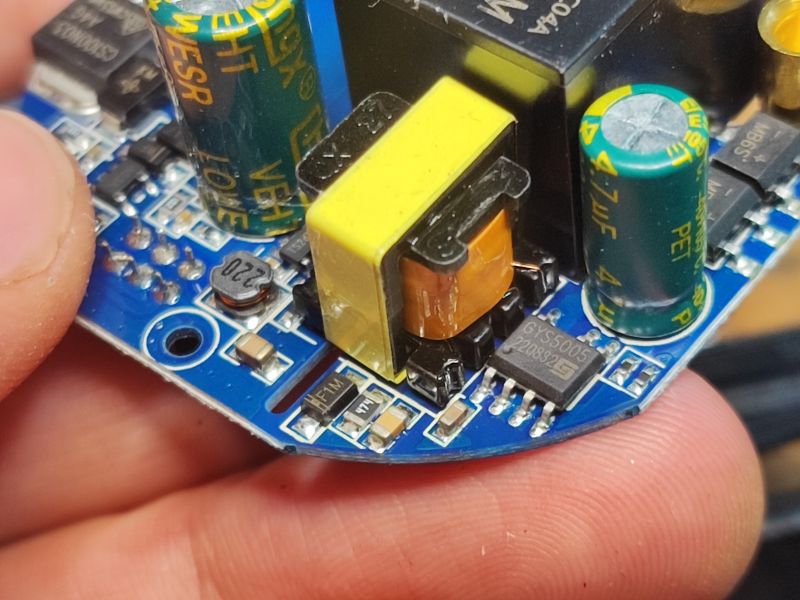
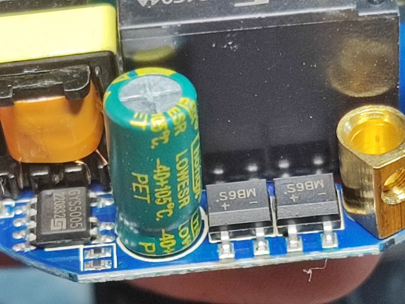
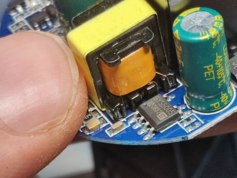
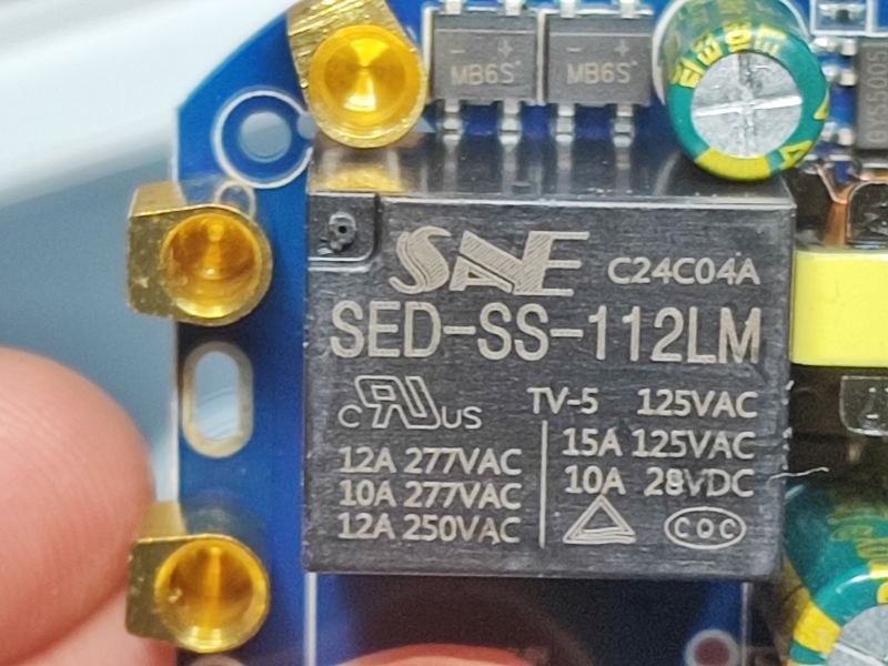
The power supply appears to be based on a GYS5005 220832, and I can also see a small step-down converter next to it, but the 3.3V LDO is not there. However, the CS100N03 (MOSFET) seems to be there so that you can also run the switch in "no neutral" mode, this will come in handy if you don't have an N wire in the box....
I've made attempts to change the firmware, at first I was hoping these pads were the UART port from the T34:
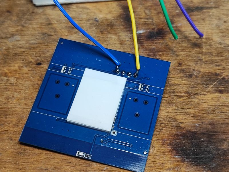 .
.
None of this, no communication. I checked the connections under the button controller:
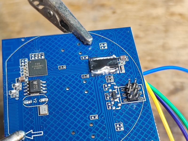
 .
.
Two of the pads lead to its feet (the other two are power and ground):
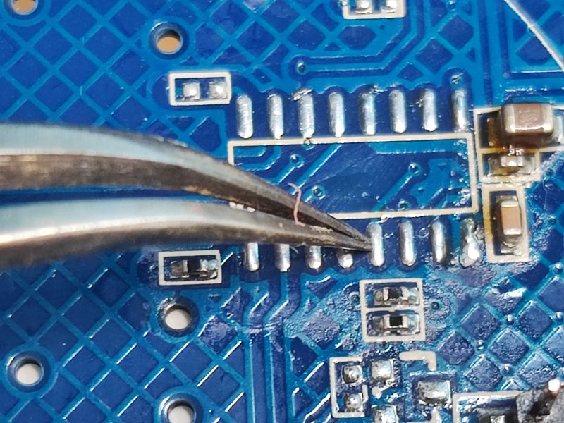
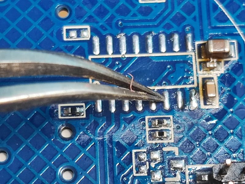 .
.
I finally debugged the T34.
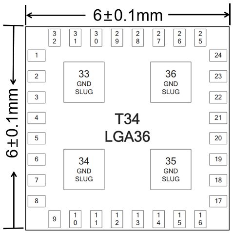 .
.
T34 outputs, quote from documentation, untranslated:
| Pin no. | Symbol | I/O type | Description | |
| 1, 3, 32, 33, 34, 35, and 36 | GND | P | Ground pins. 33, 34, 35, and 36 are the ground pads at the back of the chip. | |
| 2 | . ANT | I/O | External antenna with 2.4 GHz RF input and output. | |
| 4 and 5 | VCCPA | P | RF PA power input. Voltage range: 3.0V to 3.6V. And 3.3V power supply is recommended. | |
| 6 | . VDDDIG | O | Digital power output. The voltage is about 1.2V. | |
| 7 | . VDDAON | O | Normally open power output. The voltage is about 1.2V. | |
| 8 | VBAT | I | Chip main-.power input. Voltage range: 3.0V to 3.6V. And 3.3V power supply is recommended. | |
| 9 | . CEN | I | The CEN pin of the chip, without a reset function. This pin is floating inside the chip. | |
| 10 | . P28/ADC4/RXEN | I/O | GPIO or ADC4 or set high during RF reception. | |
| 11 | P14/SD_CLK/SCK/ANT0 | I/O | GPIO, or CLK of SD, or SCK of SPI, or Bluetooth LE antenna control ANT0. | |
| 12 | . P16/SD_CMD/MOSI/ANT2 | I/O | GPIO, or CMD of SD, or MOSI of SPI, or Bluetooth LE antenna control ANT2. | |
| 13 | .P15/CSN/ANT1 | I/O | GPIO, or CSN of SPI, or Bluetooth LE antenna control ANT1. | |
| 14 | .P17/SD_D0/MISO/ANT3 | I/O | GPIO, or D0 of SD, or MISO of SPI, or Bluetooth LE antenna control ANT3. | |
| 15 | .P26/ADC1/IRDA/PWM5 | I/O | GPIO, or ADC1, or IR receiver or PWM5. | |
| 16 | . P24/ADC2/LPO_CLK/PWM4 | I/O | GPIO, or ADC2, or low power clock 32.768K output, or PWM4. | |
| 17 | P23/ADC3/TDO/F_SO | I/O | GPIO, or ADC3, or JTAG TDO, or flash data output when downloading with SPI. | |
| 18 | . P22/ADC5/CLK_26M/TDI/TXEN/F_SI | I/O | <br/GPIO, or ADC5, or crystal frequency output, or JTAG TDI, or set high during RF transmission, or flash data input when downloading with SPI. | |
| 19 | .P21/ADC6/I2C1_SDA/TMS/F_CSN | I/O | Mode selection pin for selecting RF test firmware or app firmware. Pulling down this pin will enter the RF test mode. | |
| 20 | . P20/I2C1_SCL/TCK/F_SCK | I/O | GPIO, or SCL of I2C1, or TCK of JTAG, or the clock when flash is downloaded by SPI. | |
| 21 | .P6/CLK13M/PWM0 | I/O | GPIO, or 1, 2, 4, and 8 frequency division output of crystal clock, or PWM0. | |
| 22 | .P7/WIFI_ACTIVE/PWM1 | I/O | GPIO, or WIFI_ACTIVE control when Wi-Fi and Bluetooth coexist, or PWM1. | |
| 23 | P8/BT_ACTIVE/PWM2 | I/O | GPIO, or BT_ACTIVE control when Wi-Fi and Bluetooth coexist, or PWM2. | |
| 24 | P9/BT_PRIORITY/PWM3 | I/O | GPIO, or BT_PRIORITY control when Wi-Fi and Bluetooth coexist, or PWM3. | |
| 25 | .P10/DL_RX/UART1_RXD | I/O | GPIO, or RXD when downloading flash with UART, or RXD of serial port UART1. | |
| 26 | .P11/DL_TX/UART1_TXD | I/O | GPIO, or TXD when downloading flash with UART, or TXD of serial port UART1. | |
| 27 | P1/UART2_RXD/I2C2_SDA | I/O | GPIO, or RXD of serial port UART2, or SDA of I2C2. P1 is used for self-calibration and cannot be used for other functions. | |
| 28 | . P0/UART2_TXD/I2C2_SCL | I/O | GPIO, or TXD of serial port UART2, or SCL of I2C2. | |
| 29 | .XI | I | T34 has a build-in crystal, and no external crystal is required. | |
| 30 | XO | O | T34 has a build-in crystal, and no external crystal is required. | |
| 31 | .VSYS | O | System power output. Voltage range: 2.7V to 3.0V. |
The UART can be seen here, to the right of the photo:
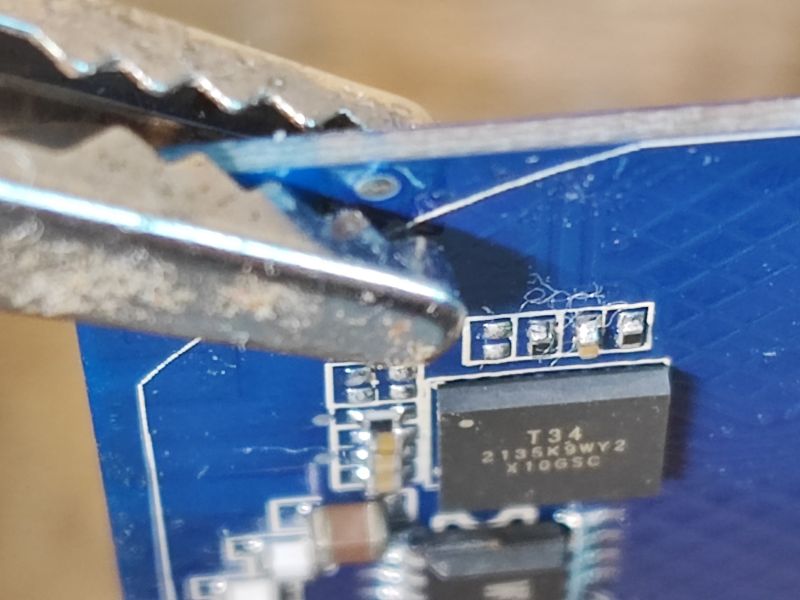 .
.
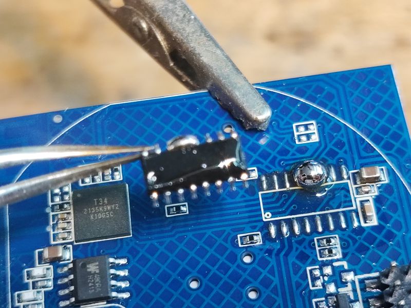
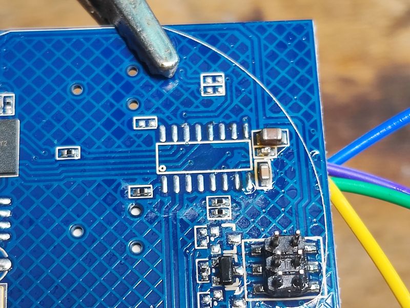
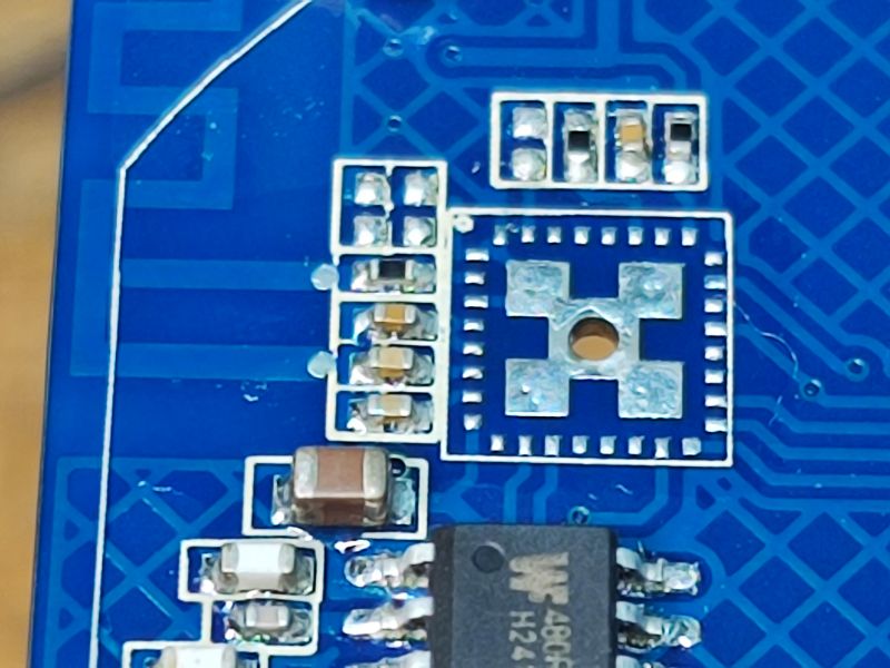
I finally desoldered the component:
 .
.
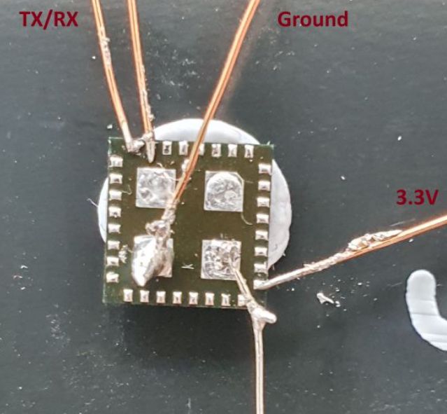
Unfortunately, it looks like pin 26 (UART1_TXD) is not brought out anywhere, so changing the firmware is difficult to access .
You will need to use the method from here:
[BK7231N / T34] Teardown Tuya Generic Wifi Wall Switch 3-fold .
CameronDev wrote:.
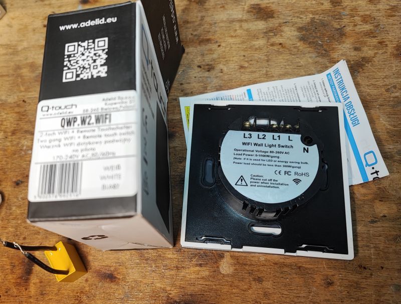
Version "double" - still just for principle, just a glance:
 .
.
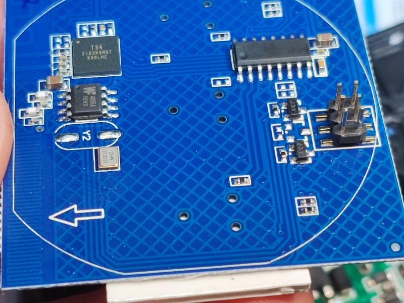
Same situation:
 .
.
The power supply is on the MT2513 ASX034N:
But that's the least of it...
In summary , the older QTouch used the ESP series, it was relatively simple to upload Tasmota. Now QTouch have a board with T34, that is with BK7231N. OpenBeken can be uploaded, but access to programming is difficult. One of the UART pins is not routed out at all. You either have to add a fine wire to the case pad itself, or solder the chip itself off the board, as shown in the linked topic. Only then can you use our flasher and connect the switch to the Home Assistant 100% locally, without the cloud.
I'll try to show the whole process separately in a dedicated topic, especially as it's undoubtedly more difficult than what has been presented so far, i.e. soldering with cables to the pads of modules such as CB2S or CB3S....
Let's hope this is an isolated incident, as changing the firmware in such a situation is more time consuming to say the least and without hot air, not a move.
And for more information on changing the T34 batch, I refer you to our search engine on elektroda.com: https://www.elektroda.com/rtvforum/find.php?q=T34
Cool? Ranking DIY Helpful post? Buy me a coffee.


