 .
.
In the previous section I showed how a beginner can get transistors for free from old scrap PC motherboards. Here I will show how to use them in practice. We will drive the MOSFET transistors from 3.3V and, in the process, see the importance of the voltage at the gate of the transistor. Here we will make the hardware basis for our own ESP8266-based WiFi-controlled dimmer.
See the previous part: Good MOSFET transistors at 5V for free? Recovering parts from an old PC motherboard .
A similar project has already been published, but there it was controlled from the 5V level so there were no combinations:
PIC12F683 and SDCC - tutorial - we create a simple dimmer (read datasheet notes) .
Free transistors and desoldering them with a regular soldering iron .
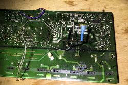
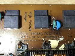
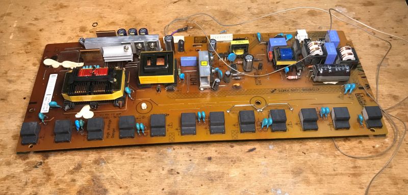
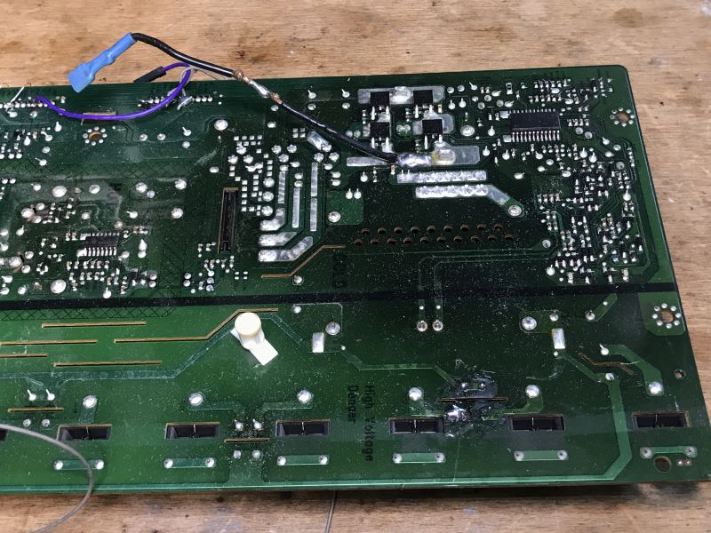
This time I found an old flat screen TV, still with fluorescent backlighting. Time for a quick visual inspection of the backlight module, which had already arrived to me damaged anyway:
 .
.
 .
.
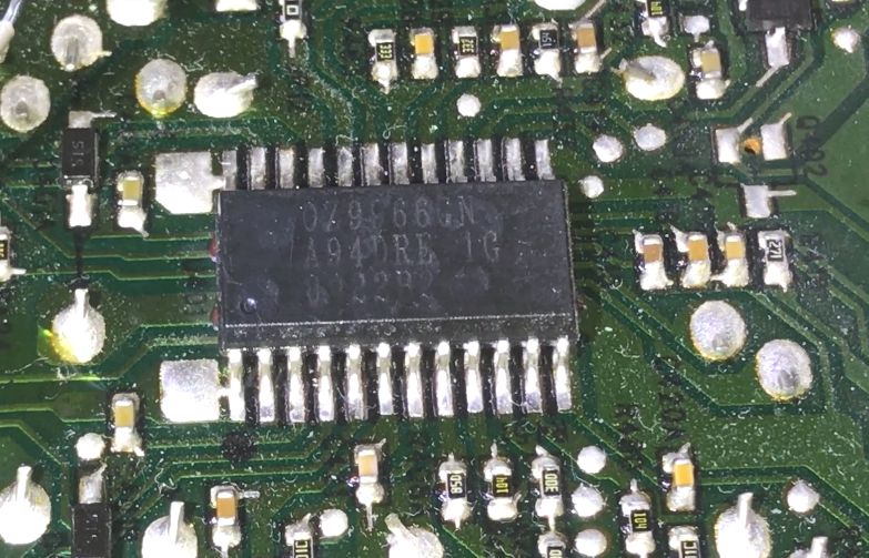
Four promising transistors can be seen at the bottom:

KMB054N40, N-type channel MOSFET, Vds=40V (drain-source voltage), Id = 54A

Resistance in the open state at Vgs=4.5V (gate voltage) not bad either, only up to 11mΩ.
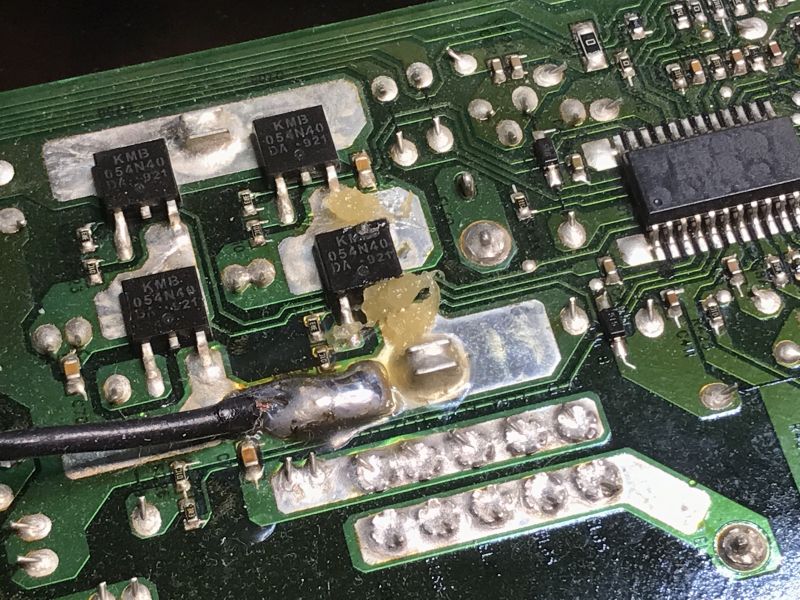
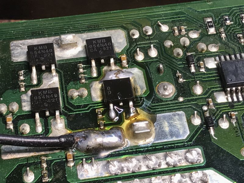
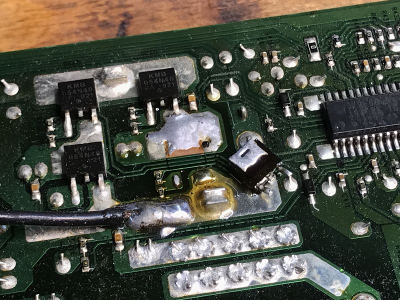
They just need to be soldered out. This can be done without hot air. My method is first flux, then lead binder on the solder to soften it, then alternate heating of the ground pours. The transistor can be removed with tweezers.
 .
.
 .
.
 .
.
Dimmer program on ESP8266 (NodeMCU here) .
I programmed the ESP8266 in PlatformIO based on ArduinoOTA so that I could upload the batch over WiFi:
How do I program the Wemos D1 (ESP8266) board in Arduino shape? ArduinoOTA in PlatformIO .
PWM - Pulse Width Modulation, pulse width modulation - is used to control brightness. Basically, we quickly "turn on and off" a logic state on a pin, here 0V or 3.3V. In Arduino, the analogWrite function is used for this. I made my program to simply dim from 0 to 100% in a loop, while refreshing the ArduinoOTA so I could still update the program over WiFi:
Code: C / C++
I expose the PWM to the GPIO2 pin, which is D4 on the NodeMCU.
Result:
The program works, and the PWM is both on the LED on the ESP12 board, and on D4.
Dimmer on KMB054N40 .
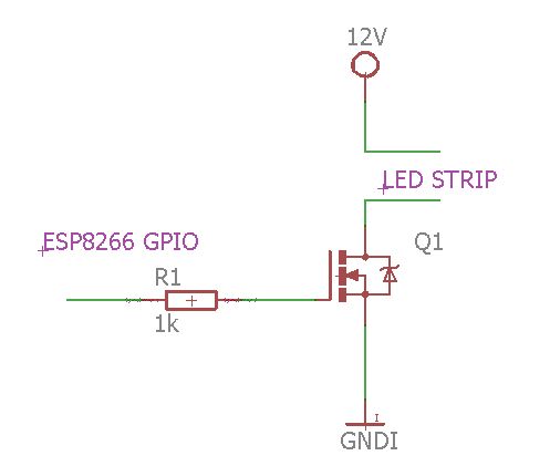
The first schematic that comes to mind is probably to connect the output of the ESP to the gate of the transistor, preferably through some sort of resistor. I've decided to start with that, although I can't say it's the correct approach. We'll see.
 .
.
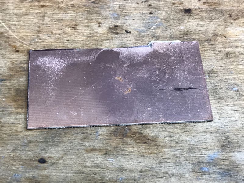
The recovered MOSFET is surface mounted, so we won't use a contact board. Anyway, I would advise against a "contact board" for higher currents. Instead, we will make a so-called 'sculpture', as some people colloquially say, on a piece of laminate. I start the process of creating such a board by cleaning the surface of the laminate so that it is easier to solder:
 .
.
 .
.
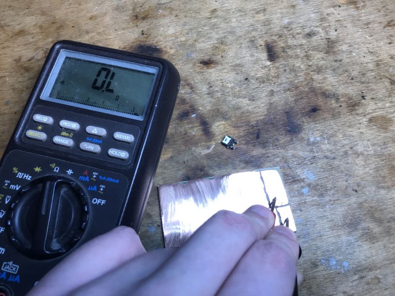
I make the breaks with a grinder, then test if there is a short circuit with a multimeter:
 .
.
 .
.
When assembling, it is worth remembering that the entire circuit must share a common ground. In addition, respect the maximum input voltage of our module from the ESP, 12V can damage it. This is the case with the NodeMCU. To power it from 12V, you will need a step-down converter, but that's off topic....
Getting started:
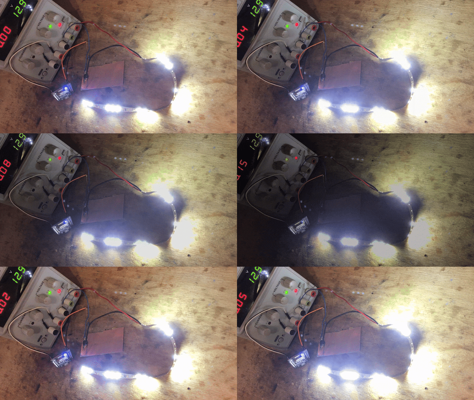 .
.
It looks like everything is working. The MOSFET does not heat up excessively....
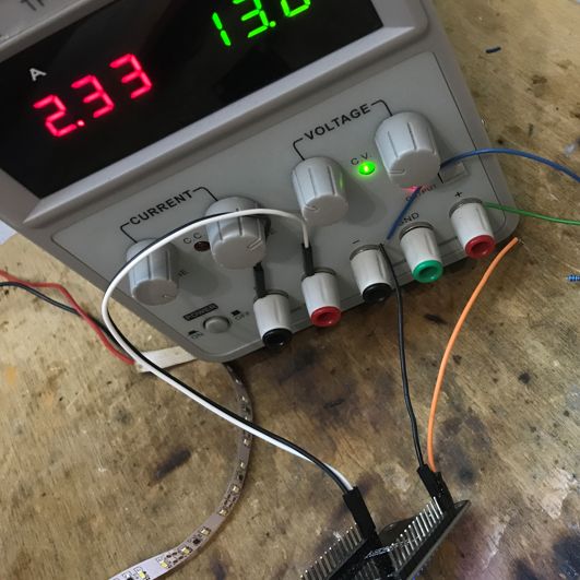
I also connected a resistor from the gate to 3.3V instead of the PWM output, it flows 2.3A, still without excessive heating:
 .
.
Dimmer on 2SK3918 .
Only is it always so colourful? Let's find out. Let's replace our KMB054N40 with the 2SK3918 I have from the topic about old PC motherboards .
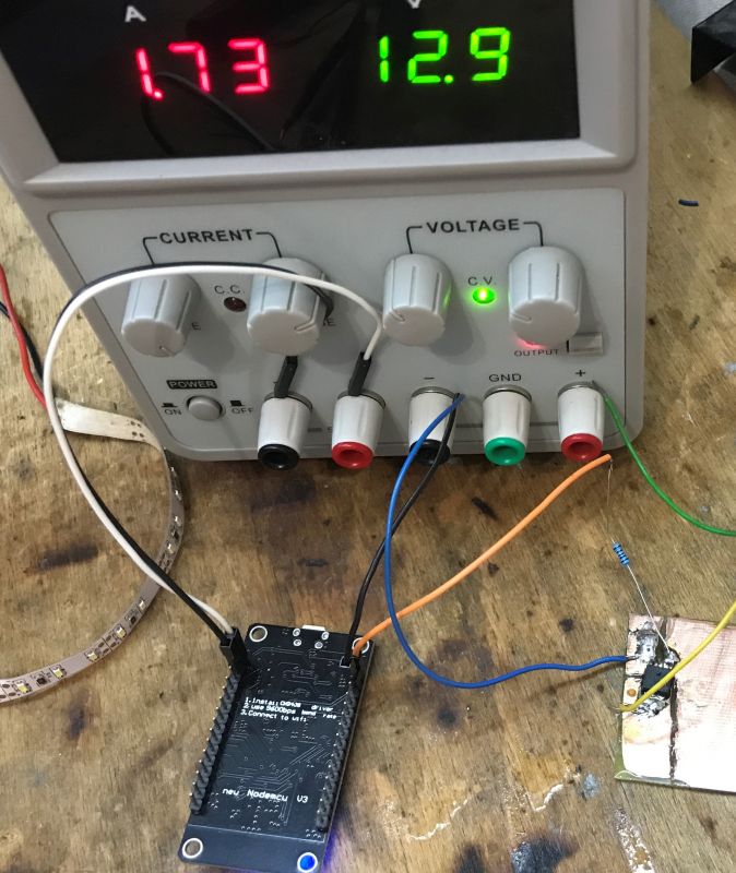
The pinouts match. Swap done, boot up and:
 .
.
Something has reduced the current, it's already strange. It was 2.3A and it's 1.73A, the LEDs are not so bright anymore, but that's not the only problem.
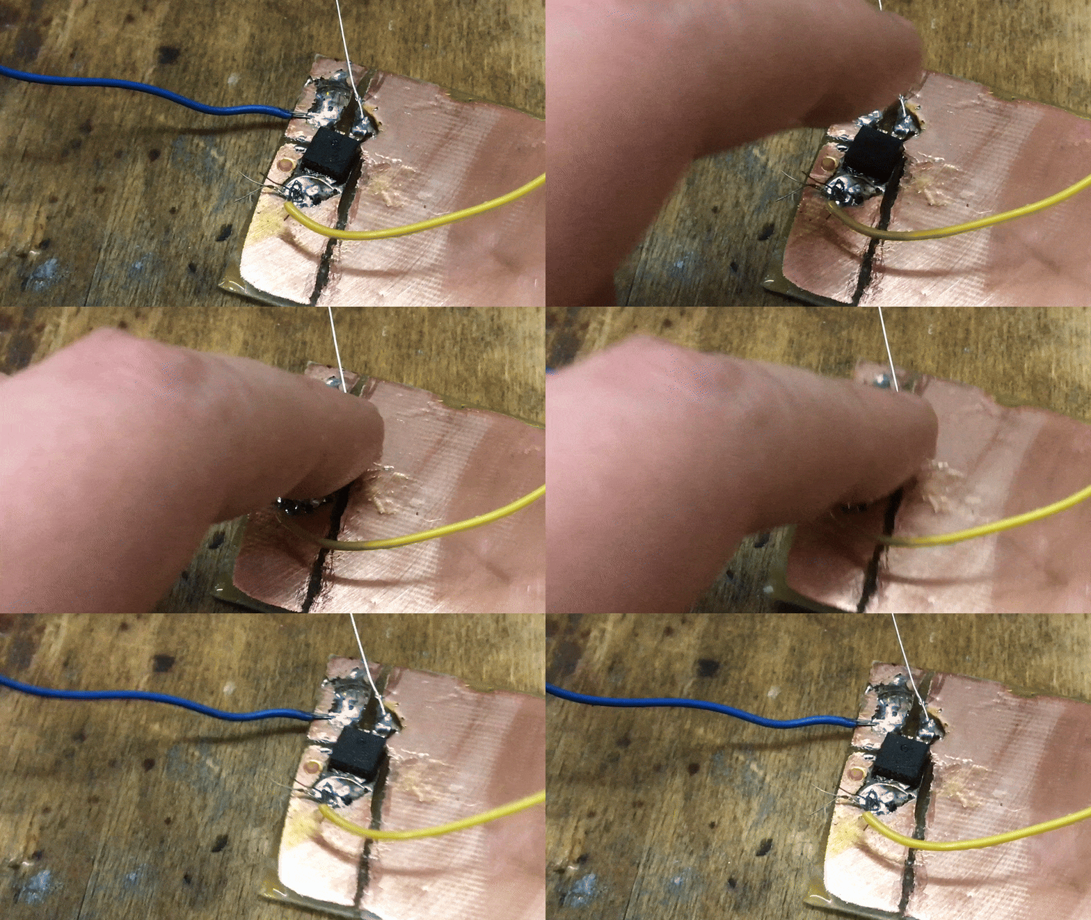
The transistor heats up and after a while it is already very warm:
 .
.
Why did the KMB054N40 manage and the 2SK3918 no longer does? .
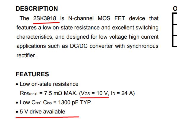
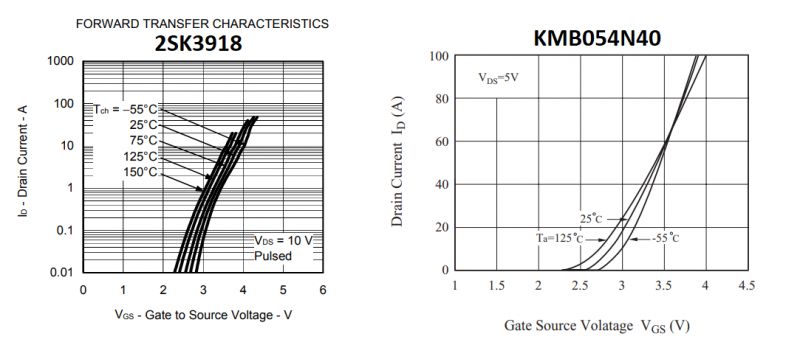
It all comes down to the control of the transistor. This is a MOSFET transistor, it is controlled by voltage. The voltage at the gate (relative to the source) is determined by the parameter Vgs. How much current will be passed through the drain (resistance in the open state) depends precisely on Vgs. This is detailed on the first page of the datasheet note, but we should actually check the diagrams as well:
 .
.
 .
.
The graphs show the drain current as a function of gate voltage, in addition with separate curves for different temperatures:
 .
.
As you can see, the 2SK3918 will fail in our circuit, i.e. at Vgs = 3.3V and at the current we expect. No wonder, it does not open fully and the resistance is too high, as a result of which it heats up. With the KMB054N40 it is slightly better, although still Vgs could be higher there.
Of course, in practice there are more dependencies here, although even on the posted graphs you can see that the junction temperature itself also has an influence (and worse, the higher the temperature, the worse the conduction), but this was supposed to be a simplified presentation so we won't go that deep.
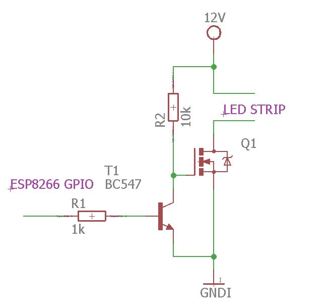
Now this needs to be fixed somehow. We need to give the gate of the MOSFET a higher voltage. The easiest way will be to add another control stage, this time a current-controlled transistor, I will find some small signal-controlled NPN. This will short the gate of the MOSFET to ground, which I will additionally pull up to 12V.
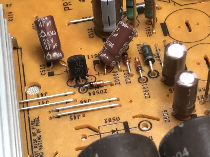
Need to search the boards again to see what is available. On the board from the inverter I saw the TL431 itself in a case in TO-92, but it's not even a transistor, but a "programmable Zener diode"... so I looked on another board, this time the power supply module, well bingo:
 .
.
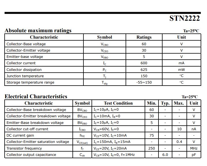
STN2222 is a small NPN bipolar transistor, the parameters look promising:
 .
.
Planned circuit:
 .
.
Just a note - now when the ESP output is 3.3V (logic 1), current flows through R1 to the base of the auxiliary transistor, causing it to open. The open auxiliary transistor then short-circuits the gate of the MOSFET to ground, simultaneously closing it. So here we have the logic reversed, but since we are writing the software for the ESP ourselves this is not a problem.
Implementation:
 .
.
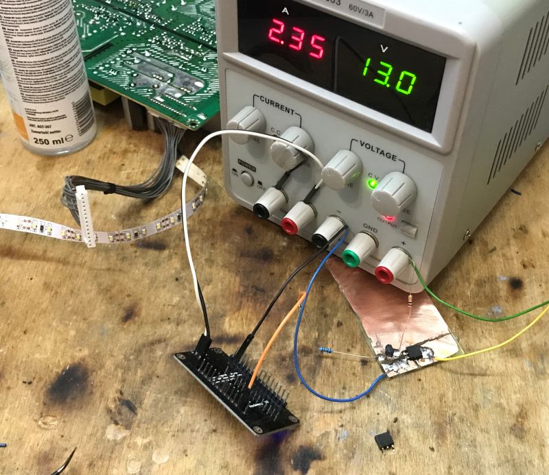
Time to check our work. This time the logic is reversed, so I connected the resistor to ground. You can immediately see that more current is flowing - almost the same as with the previous transistor, 2.3A:
 .
.
We wait, we wait and ... The MOSFET continues to be cool. Success.
I also checked the control from NodeMCu and it continues to work, we can continue to control the brightness of the LED bar.
Looks like problem solved. Maybe we can even do without a heatsink - the copper plate also dissipates some heat.
Of course, this is not the only way to control a MOSFET transistor, a lot depends on the switching frequency, gate charge, there are also dedicated drivers, but for a simple dimmer, the circuit shown here fully copes.
Summary .
This short practical demonstration showed us the importance of reading the catalogue notes of the components we intend to use in our projects. The two transistors are quite similar, but the devil is in the detail - one still somehow managed to drive from 3.3V (Vgs) at 2.3A current (Id), while the other one got excessively hot. Fortunately, we were able to fix this, even while maintaining the theme of the game - that is, selecting components from electro-waste. A side effect of this approach is that the control logic is reversed, but this is not a problem when programming such a dimmer from 0.
Now, we can take it easy on the circuit, improve the board, add some buttons, and program everything in PlatformIO with a suitable web page for control and perhaps automation (e.g. gradual lighting at a given time according to NTP time from the web).
Finally, I have allowed myself some minor simplifications in the topic, but I don't think this is a problem, in fact I hope that such a presentation will encourage beginners to experiment more with transistors.
Have you encountered a similar problem in your own projects, and if so, how did you solve it?
Cool? Ranking DIY Helpful post? Buy me a coffee.


